Follow “Electronic Engineering Magazine” and add the editor on WeChat
Regional groups are now open, please send messages 【Shenzhen】【Shanghai】【Beijing】【Chengdu】【Xi’an】 to the public account
As semiconductor technology enters the 2nm era, a global race for technological breakthroughs, market positioning, and commercial implementation is underway. In July 2025, MediaTek announced that its 2nm chip will complete tape-out in September, while Samsung aims for “global first launch,” planning to equip its Galaxy S26 series with a self-developed 2nm chip. TSMC has already started accepting 2nm orders, and major terminal players like Qualcomm and Apple are also accelerating their layouts. This struggle around the 2nm process may become a critical juncture in 2026 for this advanced technology to transition from the laboratory to large-scale commercial use.
Samsung: Betting on First Launch, Yield Challenges Ahead
As one of the few manufacturers capable of developing 2nm technology, Samsung is racing to achieve the “first launch” label. On July 30, a digital blogger revealed that the Samsung Exynos 2600 chip has entered the quality testing phase, with plans to complete verification based on the HPB solution by October 2025. If progress goes smoothly, mass production will be initiated immediately, with the Galaxy S26 series being the first to feature it.

This Exynos 2600 chip is significant—it is the world’s first 2nm mobile chip, built on Samsung’s self-developed SF2 process, and is also Samsung’s first-generation 2nm product.
Notably, the Galaxy S26 series will continue the “dual-platform” strategy, offering both the Exynos 2600 version and a version equipped with the Snapdragon 8 Elite 2. This strategy paves the way for the first launch of the 2nm chip while also allowing room to address technological risks.
However, Samsung’s path to 2nm is not smooth, as yield issues remain its biggest challenge. Data shows that Samsung’s 2nm process employs a third-generation GAA architecture and BSPDN back power delivery network technology, theoretically improving performance by 12% compared to 3nm, reducing power consumption by 25%, and shrinking chip area by 5%. However, the current trial production yield is only 30-40%, far below TSMC’s 60% yield for 2nm processes (some data indicates close to 70-80%). Even for the Tesla AI6 chip using the SF2 process, the yield is only 40-45%, lagging behind TSMC’s N2 at 70% and Intel’s 18A at 50-55%.
Despite this, Samsung is still expanding the application scenarios for 2nm. On July 28, Samsung reached a multi-year agreement worth $16.5 billion with Tesla to produce the next-generation AI6 chip at its new factory in Texas, which is expected to go into mass production in 2027, also using the SF2 process. Tesla CEO Elon Musk stated that he would personally participate in improving production efficiency, and this collaboration is seen as Samsung’s attempt to explore a new business model of “customer participation in manufacturing”.
TF Securities analyst Ming-Chi Kuo believes that the collaboration with Samsung creates a great opportunity for Tesla and Musk to participate in the wafer foundry business at a very low cost. If it were TSMC, the company would not accept such requests. The collaboration not only enhances chip design capabilities (especially in terms of manufacturability) but also, due to a better understanding of manufacturing technical know-how, will help improve Tesla’s bargaining power with foundries in the future. Musk’s various ventures will increasingly use more advanced chips, and in the long run, mastering more core technologies in chip manufacturing will be a strategic advantage.
“If the production of AI6 does not meet expectations, the worst-case scenario for Tesla is to transfer the order back to TSMC and bear the impact of delays in AI6. For Samsung, the current situation is already the worst, and it cannot get worse, so it might as well give it a try. Therefore, this collaboration is manageable risk for both parties, and if successful, both will benefit significantly.”
TSMC: Leading in Yield, Competing for High-End Orders
In the 2nm race, TSMC holds a first-mover advantage with stable yields and a solid customer base. On March 31, 2025, TSMC held a ceremony for the expansion of its 2nm production in Kaohsiung and officially began accepting 2nm wafer orders on April 1, becoming the world’s first foundry to initiate preparations for 2nm mass production.
TSMC Chairman C.C. Wei revealed that market demand for 2nm technology has surpassed that for 3nm, with potential customers including industry giants like Apple, AMD, Intel, and Broadcom. Among them, Apple is seen as the most core partner—expected to launch the A20 processor for the iPhone 18 series in the second half of 2026, which will be the global first to utilize TSMC’s 2nm process, marking Apple’s first application of the most advanced technology in mobile chips.
On a technical level, TSMC’s 2nm process yield has reached 60%, far exceeding Samsung’s 30-40%, which means it can achieve large-scale production at a lower cost. However, the high cost of 2nm chips remains a significant issue: the cost of a single 2nm wafer is about $30,000, and when factoring in the costs of building factories in the U.S. and tariffs, the prices of end products may rise, ultimately borne by the supply chain and consumers.
In addition to Apple, Qualcomm is also rumored to plan to adopt TSMC’s 2nm process. Although Qualcomm has collaborated with Samsung to develop the Snapdragon 8 Elite Gen 2 based on the 2nm process (designed for Samsung’s foldable phones, set to launch in the third quarter of 2026), the industry generally believes that its flagship chips will still likely choose TSMC for foundry services to balance performance and yield.
MediaTek: Dual Breakthroughs from Mobile to Cloud
MediaTek’s performance in the 2nm race is also impressive, showing a dual-track approach of “mobile + cloud”. On July 30, MediaTek CEO Rick Tsai announced at a press conference that the company’s 2nm chip is expected to complete design finalization (tape-out) by September 2025, with plans for commercial use in 2026, making it one of the first manufacturers to launch a 2nm chip.
In the mobile sector, MediaTek’s flagship chip business is growing rapidly. Tsai expects that revenue from the Dimensity flagship mobile chip will reach $3 billion in 2025, a year-on-year increase of over 40%. The Dimensity 9500 chip, which is set to go into mass production in the third quarter, will further strengthen its presence in the high-end mobile market. The development of the 2nm chip will help it achieve leaps in performance and AI computing power, directly competing with Qualcomm and Apple.
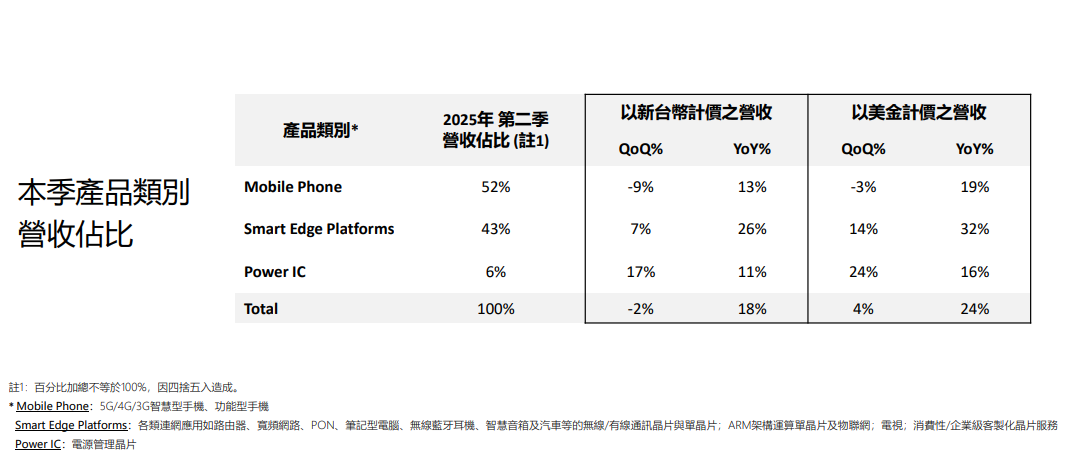
Note: MediaTek’s product category revenue share in Q2 2025
More noteworthy is MediaTek’s breakthrough in cloud ASIC chips. Recently, it was reported that MediaTek has replaced Broadcom to secure the 2nm ASIC chip order codenamed “Arke” from Meta. This chip is designed for AI inference tasks and will be used in scenarios such as smart voice assistants and image recognition, marking an important part of Meta’s adjustment of its chip strategy—from solely relying on high-end training chips to a more cost-effective and efficient scenario-based customization.
In fact, this is not MediaTek’s first breakthrough in the cloud market. Its TPU v7e chip, developed in collaboration with Google, is planned for mass production by the end of 2026, expected to contribute $1.5-2 billion in revenue in 2027, increasing to $3-4 billion in 2028-2029, accounting for over 10% of total revenue. MediaTek’s advantage lies in its ability to balance high performance with low cost, which aligns well with the current cloud service providers’ emphasis on “delivery efficiency, cost control, and ease of deployment”.
Additionally, MediaTek is also making strides in the automotive chip sector, with a smart cockpit solution C-X1 developed in collaboration with NVIDIA set to be sampled in the second half of 2025, contributing revenue starting in 2026, laying the groundwork for the diverse applications of 2nm technology.
Technology and Competition: The Core Proposition of the 2nm Era
The reason the 2nm process has become a battleground for global manufacturers is due to its disruptive performance improvements. Compared to 3nm, the 2nm process can generally achieve a 12-15% performance increase, a 20-25% reduction in power consumption, and a reduction in chip area, which is crucial for fields with surging computing power demands such as mobile, AI, and automotive.
In terms of technical pathways, GAA (Gate-All-Around) architecture has become the mainstream choice for 2nm. Samsung employs a third-generation GAA architecture and introduces BSPDN back power delivery network; TSMC, on the other hand, optimizes the transistor structure based on GAA, both attempting to break physical limits through architectural innovation.
However, yield and cost remain unavoidable challenges. Samsung’s 30-40% yield means that out of every 100 wafers produced, only 30-40 can meet commercial standards, directly driving up production costs; while TSMC’s 60% yield, though advantageous, still makes the $30,000 cost per wafer a barrier for small and medium-sized manufacturers. This explains why the initial customers for 2nm are mostly giants like Apple, Tesla, and Meta—only they can bear the high R&D and production costs and dilute expenses through large-scale shipments.
From a competitive landscape perspective, 2nm will intensify market differentiation. TSMC, with its yield and customer advantages, is likely to solidify its dominant position in the foundry market (currently holding 67% of the global share); Samsung is trying to open up the situation through collaborations with Tesla and Qualcomm, but its 8% foundry share still needs to break through; MediaTek is leveraging its dual-track approach in cloud and mobile to challenge the positions of traditional giants like Broadcom.
2026: Commercial Explosion and Industry Restructuring
As various manufacturers push forward, 2026 will be a key year for the commercial use of 2nm chips. Products such as Samsung’s Galaxy S26 series, Apple’s iPhone 18 series, MediaTek’s Dimensity 2nm chip, and Qualcomm’s Snapdragon 8 Elite Gen 2 will be launched, marking the transition of 2nm technology from the laboratory to consumer terminals.
For consumers, 2nm mobile phones may bring longer battery life, stronger AI capabilities, and smoother experiences, but price increases may be inevitable; for the industry, 2nm will accelerate the descent of AI computing power from data centers to edge devices, breaking performance bottlenecks in scenarios such as smart cars and AR/VR.
In the long run, the competition for 2nm is not only a contest of technology but also a battle for ecosystems. Manufacturers that master 2nm technology will gain greater influence in the industry chain, while those unable to keep pace may be marginalized.
In this race, whoever can first break through the yield bottleneck, balance cost and performance, and expand diverse application scenarios will seize the initiative in the 2nm era. The outcome of this contest may become apparent in the commercial wave of 2026.