Introduction to ADC
The STM32F103 series has 3 ADCs with a precision of 12 bits, and each ADC can have up to 16 external channels. ADC1 and ADC2 both have 16 external channels, while ADC3 generally has 8 external channels. The A/D conversion of each channel can be executed in single, continuous, scan, or interrupt mode. The results of the ADC conversion can be stored in a 16-bit data register, either left-aligned or right-aligned. The input clock for the ADC must not exceed 14MHz, and its clock frequency is generated by dividing PCLK2.
Explanation of ADC Functional Block Diagram
When learning about the peripherals on the STM32 development board, it is essential to understand the functional block diagram of the peripherals, as shown below:
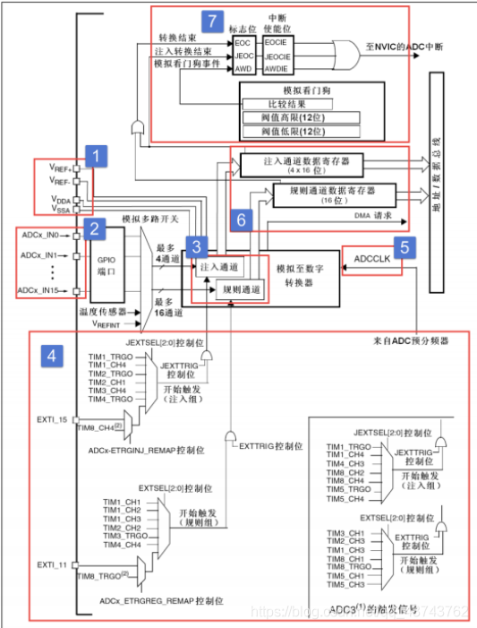
The functional block diagram can be roughly divided into 7 parts, which will be explained one by one below:
Voltage Input Range
The voltage range that the ADC can measure is VREF- ≤ VIN ≤ VREF+. By grounding VSSA and VREF-, and connecting VREF+ and VDDA to 3V3, the input voltage range for the ADC is: 0~3.3V.
Input Channels
The signal input to the ADC is achieved through channels, where the signal enters the microcontroller through the channels, and the microcontroller converts it to output a digital signal. The ADC in STM32 has 18 channels, of which the 16 external channels are marked in the block diagram below:
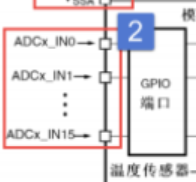
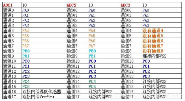
These 16 channels correspond to different IO ports. Additionally, ADC1/2/3 also have internal channels: Channel 16 of ADC1 is connected to the internal temperature sensor, and Vrefint is connected to Channel 17. The analog channels 16 and 17 of ADC2 are connected to the internal VSS.
All channels of the ADC are shown in the figure below:
The 16 external channels are further classified into regular channels and injected channels during conversion. The regular channels can have up to 16 paths, while the injected channels can have up to 4 paths (injected channels seem to be used less frequently). Below is a brief introduction to the two types of channels:
As the name suggests, regular channels are the most common and frequently used channels, and ADC conversions are typically performed using regular channels.
Injected channels are relative to regular channels; they can forcibly interrupt the conversion of regular channels, similar to an “interrupt channel.” When an injected channel needs to be converted, the conversion of the regular channel will stop, and the conversion of the injected channel will take precedence. After the conversion of the injected channel is completed, the system will return to the previous regular channel for conversion.
Conversion Order
After understanding the ADC conversion channels, if the ADC only uses one channel for conversion, it is straightforward. However, if multiple channels are used for conversion, it involves a sequence of operations, as there is only one data register for regular conversion channels. The order of multiple channel usage is divided into two cases: the conversion order of regular channels and the conversion order of injected channels.
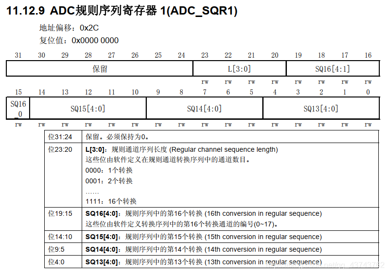
The conversion order in regular channels is controlled by three registers: SQR1, SQR2, and SQR3, all of which are 32-bit registers. The SQR registers control the number of conversion channels and the conversion order. By writing the corresponding channel into the SQx bit of the corresponding register, that channel becomes the x-th conversion. The specific correspondence is as follows:
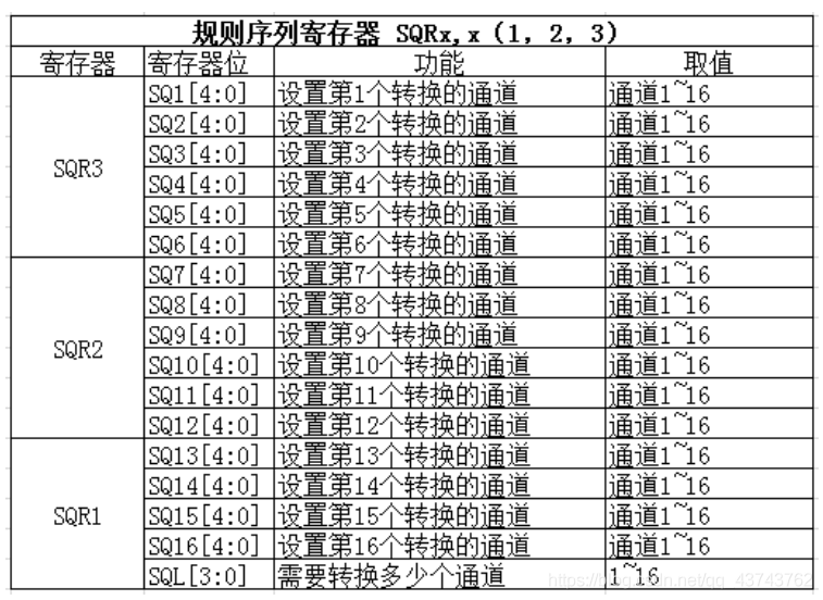
The conversion order can be understood through the SQR1 register implementation:
Similar to the control of the conversion order of regular channels, the conversion of injected channels is also controlled by an injected register, but there is only one JSQR register for control, and the control relationship is as follows:
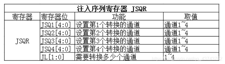
It is important to note that the conversion order of injected channels will only be executed in the order of JSQ1, JSQ2, JSQ3, JSQ4 when JL=4. When JL<4, the conversion order of injected channels is executed in reverse order: JSQ4, JSQ3, JSQ2, JSQ1.
The function to configure the conversion order is shown in the following code:
/** * @brief Configures for the selected ADC regular channel its corresponding * rank in the sequencer and its sample time. * @param ADCx: where x can be 1, 2 or 3 to select the ADC peripheral. * @param ADC_Channel: the ADC channel to configure. * This parameter can be one of the following values: * @arg ADC_Channel_0: ADC Channel0 selected * @arg ADC_Channel_1: ADC Channel1 selected * @arg ADC_Channel_2: ADC Channel2 selected * @arg ADC_Channel_3: ADC Channel3 selected * @arg ADC_Channel_4: ADC Channel4 selected * @arg ADC_Channel_5: ADC Channel5 selected * @arg ADC_Channel_6: ADC Channel6 selected * @arg ADC_Channel_7: ADC Channel7 selected * @arg ADC_Channel_8: ADC Channel8 selected * @arg ADC_Channel_9: ADC Channel9 selected * @arg ADC_Channel_10: ADC Channel10 selected * @arg ADC_Channel_11: ADC Channel11 selected * @arg ADC_Channel_12: ADC Channel12 selected * @arg ADC_Channel_13: ADC Channel13 selected * @arg ADC_Channel_14: ADC Channel14 selected * @arg ADC_Channel_15: ADC Channel15 selected * @arg ADC_Channel_16: ADC Channel16 selected * @arg ADC_Channel_17: ADC Channel17 selected * @param Rank: The rank in the regular group sequencer. This parameter must be between 1 to 16. * @param ADC_SampleTime: The sample time value to be set for the selected channel. * This parameter can be one of the following values: * @arg ADC_SampleTime_1Cycles5: Sample time equal to 1.5 cycles * @arg ADC_SampleTime_7Cycles5: Sample time equal to 7.5 cycles * @arg ADC_SampleTime_13Cycles5: Sample time equal to 13.5 cycles * @arg ADC_SampleTime_28Cycles5: Sample time equal to 28.5 cycles * @arg ADC_SampleTime_41Cycles5: Sample time equal to 41.5 cycles * @arg ADC_SampleTime_55Cycles5: Sample time equal to 55.5 cycles * @arg ADC_SampleTime_71Cycles5: Sample time equal to 71.5 cycles * @arg ADC_SampleTime_239Cycles5: Sample time equal to 239.5 cycles * @retval None */void ADC_RegularChannelConfig(ADC_TypeDef* ADCx, uint8_t ADC_Channel, uint8_t Rank, uint8_t ADC_SampleTime){ // Function content omitted;}Trigger Sources
The input, channel, and conversion order of the ADC conversion have been explained, but how is the ADC conversion triggered? Just like communication protocols, a start signal is required to transmit information; the ADC also needs a trigger signal to perform analog-to-digital conversion.
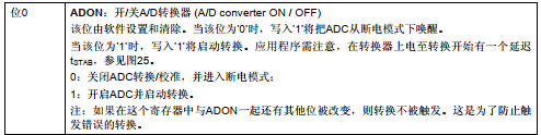
One way is to trigger it by directly configuring the register. By configuring the ADON bit of control register CR2, writing 1 starts the conversion, and writing 0 stops the conversion. During program execution, simply calling the library function to set the ADON bit of the CR2 register to 1 allows conversion, which is quite straightforward.
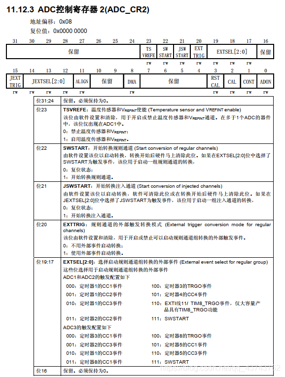
Additionally, conversion can also be triggered by an internal timer or external IO, meaning that the internal clock can be used for periodic conversion, or external IO can trigger the ADC when needed. The specific trigger is determined by control register CR2.
The details of the ADC_CR2 register can be found in the reference manual, as shown below:
Conversion Time
Another point is the issue of conversion time; each signal conversion of the ADC takes time, which is the conversion time determined by the input clock and sampling period.
Since the ADC in STM32 is mounted on the APB2 bus, its clock is derived from PCLK2 (72MHz) through division. The division factor is set by the RCC clock configuration register RCC_CFGR bits 15:14 ADCPRE[1:0], which can be set to 2/4/6/8 division. Generally, the division factor is set to 8, which gives an input clock frequency of 9MHz for the ADC.
The sampling period is determined based on the input clock. Configuring the sampling period can specify how many ADC clock cycles to sample the voltage. The number of sampling cycles can be set through the ADC sampling time registers ADC_SMPR1 and ADC_SMPR2 in the SMP[2:0] bits. ADC_SMPR2 controls channels 0~9, and ADC_SMPR1 controls channels 10~17. Each channel can be configured with different sampling periods, but the minimum sampling period is 1.5 cycles. This means that if you want to sample as quickly as possible, set the sampling period to 1.5.
Conversion Time = Sampling Time + 12.5 CyclesThe 12.5 cycles is fixed. Generally, we set PCLK2=72M, and through the ADC prescaler, the maximum clock that can be divided is 12M. When the sampling period is set to 1.5 cycles, the shortest conversion time is calculated to be 1.17us.
Data Registers
The data after conversion is stored in data registers, but the storage is also divided into data for regular channel conversions and data for injected channel conversions.
The regular data register is responsible for storing data from regular channel conversions, stored through the 32-bit register ADC_DR:
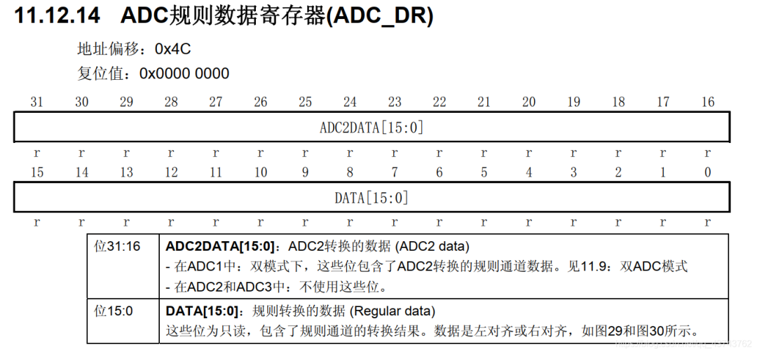
When using ADC in independent mode (i.e., using only one ADC, but can use multiple channels), the data is stored in the lower 16 bits. When using ADC in multi-mode, the high 16 bits store data from ADC2. It is important to note that the precision of ADC conversion is 12 bits, while the register has 16 bits to store data, so it must be specified whether the data is stored left-aligned or right-aligned.
When using multiple channels for conversion, multiple conversion data will be generated. However, since there is only one data register, storing multiple data in one register will overwrite the data, leading to ADC conversion errors. Therefore, we often immediately retrieve the data after a channel conversion is completed to facilitate the storage of the next data. Generally, DMA mode is enabled to transfer the converted data into an array, allowing the program to read the array to obtain the conversion results.
The use of DMA has been introduced earlier; please refer to this link: DMA Introduction.
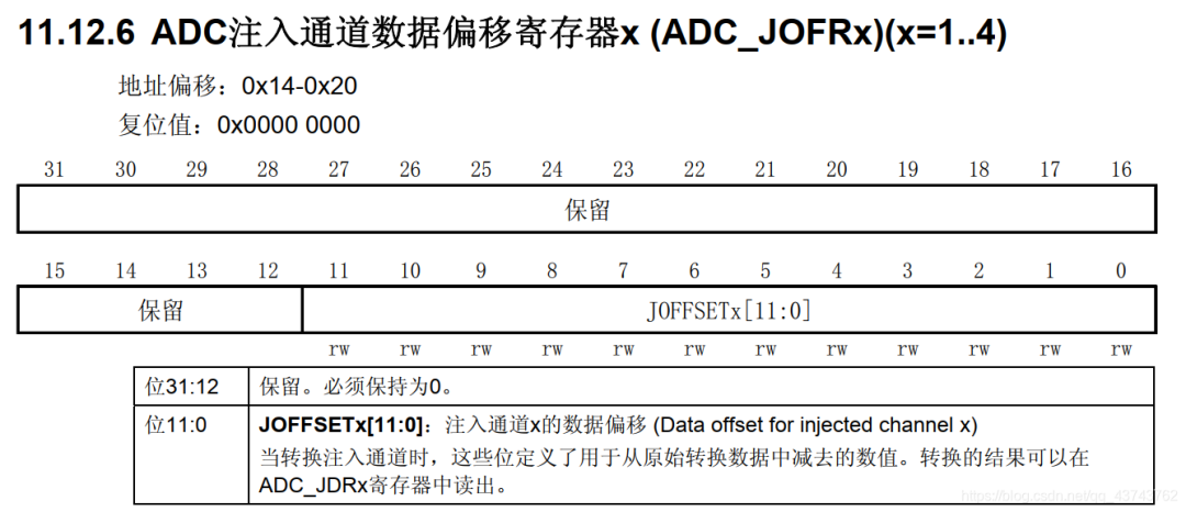
The data registers for injected channel conversions are 4 in total. Since there can be at most 4 injected channels, the data for injected channel conversions has fixed storage locations, preventing data overwriting issues like those in the regular registers. ADC_JDRx is 32 bits, with the lower 16 bits being valid and the upper 16 bits reserved. The data is also divided into left-aligned and right-aligned, with the specific storage method set by bit 11 of ADC_CR2 ALIGN.
Interrupts
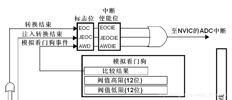 From the block diagram, it can be seen that after the data conversion is completed, interrupts can be generated in three situations:
-
After the data conversion of the regular channel is completed, an interrupt can be generated, allowing the value of the regular data register to be read in the interrupt function. This is also a method to read data when using a single channel.
-
After the data conversion of the injected channel is completed, an interrupt can be generated, and the value of the injected data register can also be read in the interrupt, achieving data reading.
-
When the input analog quantity (voltage) falls outside the threshold range, a watchdog event will be generated to monitor whether the input analog quantity is normal.
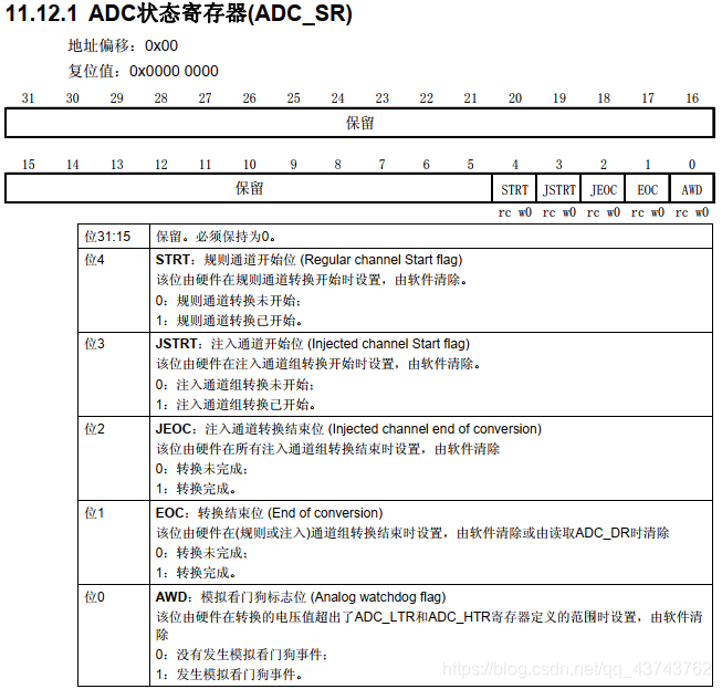
The configuration of the above interrupts is determined by the ADC_SR register:
Of course, after the conversion is completed, a DMA request can also be generated to read the converted data from the data register into memory.
Voltage Conversion
It is essential to understand that the converted data is a 12-bit binary number. We need to represent the analog quantity (voltage) that this binary number represents in numerical form. For example, if the measured voltage range is 0~3.3V, and the converted binary number is x, since the 12-bit ADC divides the voltage range size (which is 3.3) into 4096 (2^12) parts, the calculation method for the actual voltage represented by the converted binary number x is:
y=3.3* x / 4096Initialization Structure
The core of each peripheral is its corresponding initialization structure. The ADC initialization structure code is as follows:
typedef struct {uint32_t ADC_Mode; // ADC working mode selection FunctionalState ADC_ScanConvMode; // ADC scan (multi-channel) or single (single-channel) mode selection FunctionalState ADC_ContinuousConvMode; // ADC single conversion or continuous conversion selectionuint32_t ADC_ExternalTrigConv; // ADC conversion trigger signal selectionuint32_t ADC_DataAlign; // ADC data register alignment formatuint8_t ADC_NbrOfChannel; // Number of ADC acquisition channels } ADC_InitTypeDef;The ADC’s related information is set by configuring the initialization structure.
Single Channel Voltage Acquisition
Let’s use this program to simply practice the single channel voltage acquisition of the ADC. The program uses channel 11 of ADC1, corresponding to IO port PC^1. Since there is no multiplexing on the PC^1 pin of the author’s development board, it uses interrupts to read the converted voltage in the interrupt.
Header File
To improve the portability of the files, some quantities related to the ADC and interrupts are defined in the header file. When porting the program, only the definitions in the header file need to be modified.
#ifndef __ADC_H#define __ADC_H#include "stm32f10x.h"/* Using ADC1 channel 11 Pin is PC^1, mode must be analog input*/#define ADC_GPIO_RCC RCC_APB2Periph_GPIOC#define ADC_GPIO_PORT GPIOC#define ADC_GPIO_PIN GPIO_Pin_1#define ADC_GPIO_MODE GPIO_Mode_AIN /* Configuration related to interrupts */#define ADC_IRQn ADC1_2_IRQn#define ADC_RCC RCC_APB2Periph_ADC1/* Macro definitions for configuring the ADC initialization structure */#define ADCx ADC1#define ADCx_ContinuousConvMode ENABLE //Continuous conversion mode#define ADCx_DataAlign ADC_DataAlign_Right //Right alignment of conversion results#define ADCx_ExternalTrigConv ADC_ExternalTrigConv_None //No external trigger for conversion, using software trigger#define ADCx_Mode ADC_Mode_Independent //Using only one ADC, independent mode#define ADCx_NbrOfChannel 1 //One conversion channel#define ADCx_ScanConvMode DISABLE //Disable scan mode, use for multi-channel/* Channel information and sampling period */#define ADC_Channel ADC_Channel_11#define ADC_SampleTime ADC_SampleTime_55Cycles5/* Function declarations */void ADC_COnfig(void);void ADC_NVIC_Config(void);void ADC_GPIO_Config(void);void ADCx_Init(void);#endif /* __ADC_H */Pin Configuration Function
First, configure the corresponding GPIO pin, as the analog signal is transmitted to the development board through the GPIO pin. Note that the pin mode must be analog input!
void ADC_GPIO_Config(void){GPIO_InitTypeDef GPIO_InitStruct;RCC_APB2PeriphClockCmd(ADC_GPIO_RCC, ENABLE);GPIO_InitStruct.GPIO_Pin = ADC_GPIO_PIN ;GPIO_InitStruct.GPIO_Mode = ADC_GPIO_MODE ;GPIO_Init(ADC_GPIO_PORT , &GPIO_InitStruct);}Configuring the pin follows the usual routine: declare a structure variable, enable the clock, write to the structure, and initialize GPIO.
NVIC Configuration Function
Since we are using interrupts to read data after conversion, we need to configure the priority of the interrupt function. As there is only one interrupt in the program, the priority configuration is relatively flexible.
void ADC_NVIC_Config(void){NVIC_InitTypeDef NVIC_InitStruct ;/* Configure interrupt priority grouping (set allocation of preemption priority and sub-priority), in the function in misc.c */NVIC_PriorityGroupConfig(NVIC_PriorityGroup_1) ;/* Configure initialization structure in misc.h *//* Configure interrupt source in stm32f10x.h */NVIC_InitStruct.NVIC_IRQChannel = ADC_IRQn ;/* Set preemption priority */NVIC_InitStruct.NVIC_IRQChannelPreemptionPriority = 1 ;/* Set sub-priority */NVIC_InitStruct.NVIC_IRQChannelSubPriority = 1 ;/* Enable interrupt channel */NVIC_InitStruct.NVIC_IRQChannelCmd = ENABLE ;/* Call initialization function */NVIC_Init(&NVIC_InitStruct) ;}ADC Configuration Function
The ADC configuration function is the essence of the ADC. This function includes the configuration of the ADC initialization structure, clock division, channel conversion order, enabling conversion interrupts, calibration, and software-triggered ADC acquisition.
The function contains detailed comments:
void ADC_COnfig(void){ ADC_InitTypeDef ADC_InitStruct; RCC_APB2PeriphClockCmd(ADC_RCC, ENABLE);/* Configure initialization structure, see header file for details */ ADC_InitStruct.ADC_ContinuousConvMode = ADCx_ContinuousConvMode ; ADC_InitStruct.ADC_DataAlign = ADCx_DataAlign ; ADC_InitStruct.ADC_ExternalTrigConv = ADCx_ExternalTrigConv ; ADC_InitStruct.ADC_Mode = ADCx_Mode ; ADC_InitStruct.ADC_NbrOfChannel = ADCx_NbrOfChannel ; ADC_InitStruct.ADC_ScanConvMode = ADCx_ScanConvMode ; ADC_Init(ADCx, &ADC_InitStruct);/* Configure ADC clock to 8 division, which is 9M */ RCC_ADCCLKConfig(RCC_PCLK2_Div8);/* Configure ADC channel conversion order and time */ ADC_RegularChannelConfig(ADCx, ADC_Channel, 1, ADC_SampleTime );/* Enable interrupt after conversion completion, read information in interrupt */ ADC_ITConfig(ADCx, ADC_IT_EOC,ENABLE);/* Enable ADC and start conversion */ ADC_Cmd(ADCx, ENABLE );/* Reset ADC calibration */ ADC_ResetCalibration(ADCx);/* Wait for initialization to complete */while(ADC_GetResetCalibrationStatus( ADCx))/* Start calibration */ ADC_StartCalibration(ADCx);/* Wait for calibration to complete */while (ADC_GetCalibrationStatus(ADCx));/* Software trigger ADC conversion */ ADC_SoftwareStartConvCmd(ADCx, ENABLE);}Interrupt Function
In the interrupt function, data is read and stored in the variable result. The keyword extern is used here to declare that the variable result has been defined in another file. For an introduction to extern, please refer to this link: extern Keyword.
extern uint16_t resurt;void ADC1_2_IRQHandler(void){/* Check for interrupt request */while(ADC_GetITStatus(ADCx, ADC_IT_EOC) == SET) resurt=ADC_GetConversionValue(ADCx);/* Clear interrupt flag */ ADC_ClearITPendingBit(ADCx, ADC_IT_EOC);}Main Function
The main function is responsible for receiving the converted value and converting it to a voltage value, which is then printed to the computer via serial port for debugging purposes.
The variable result is a global variable in the main function, and it is important to note that the final result should be converted to a floating-point type.
#include "stm32f10x.h"#include "usart.h"#include "adc.h"uint16_t result;void delay(void){uint16_t k=0xffff;while(k--);}int main(void){float voltage;/* Serial port debug function */ DEBUG_USART_Config();/* Functions related to ADC are packed in this function */ ADCx_Init();while(1) {/* Force conversion to float */ voltage = (float) result/4096*3.3;printf("\nVoltage value: %f\n",voltage); delay(); }}