–
FM4550 Domestic Development Board
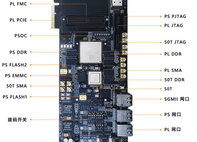
Function Interface –
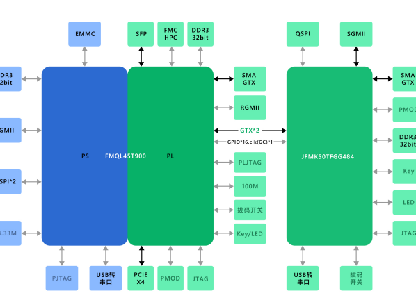
– System Block Diagram –
01
– Product Parameters –
1.
Main Parameters
System 1:
-
FPGA Model: FMQL45T900
-
PS Core: Quad-core ARM Cortex-A7, Frequency 800MHz
-
PS Memory: 1GB DDR3, Data Rate 1066Mbps, 32bit
-
PL Memory: 1GB DDR3, Data Rate 1600Mbps, 32bit
-
GTX Transceiver: 16X
-
Speed Grade: Comparable to Imported -2 Chip Level: Industrial Grade
-
Operating Temperature: -40℃-100℃ Logic Element Count: 350k
-
Lookup Table: 218600 Multiplier: 900
-
Flip-Flops: 437200 Block RAM: 19.1Mb
-
EMMC FLASH: 8GB QSPI FLASH: 128Mbit*2
System 2:
-
FPGA Model: JFMK50TFGG484
-
PL Memory: 1GB DDR3, Data Rate 1600Mbps, 32bit
-
GTX Transceiver: 4X
-
Speed Grade: Comparable to Imported -2 Chip Level: Industrial Grade
-
Operating Temperature: -40℃-100℃ Logic Element Count: 52.16k
-
Lookup Table: 8150 Multiplier: 120
-
Flip-Flops: 65200 Block RAM: 2.7Mb
-
QSPI FLASH: 128Mbit
2.
Interfaces and Functions
DDR3:
-
FMQL45T900:
-
PS Side: 2 pieces of 512MB DDR3 memory, 32bit bus, can be used as data cache and operating system running memory;
-
PL Side: 2 pieces of 512MB DDR3 memory, 32bit bus, can be used as data storage.
-
JFMK50TFGG484: Contains 2 pieces of 512MB DDR3 memory, 32bit bus, can be used as data storage.
QSPI FLASH:
-
FMQL45T900, PS side: 2 pieces of 128Mbit QSPI storage
-
JFMK50TFGG484: Contains 1 piece of 128Mbit QSPI storage.
EMMC FLASH:
-
FMQL45T900’s PS side has 1 piece of 8GB EMMC storage chip, can be used to store operating system and user data
PCIe Interface:
-
FMQL45T900 provides a standard PCIeX4 high-speed data interface, supporting PCI Express 2.0 standard.
Ethernet Interface:
-
FMQL45T900’s PS side and PL segment each have 1 Ethernet RJ-45 interface for Ethernet data exchange.
-
JFMK50TFGG484 has 1 Ethernet RJ-45 interface for Ethernet data exchange, using SGMII interface PHY.
JTAG Port:
-
FMQL45T900 has one PJTAG interface and one PLJTAG interface.
-
JFMK50TFGG484 has one JTAG interface for system downloading and debugging.
Crystal Oscillator:
-
FMQL45T900 PS side has one 33.333MHz active crystal oscillator, providing a stable clock source for the PS system. PL side has one 100MHz active crystal oscillator for additional clock supply.
FMC:
-
FMQL45T900 has one FMC HPC interface for external various FMC HPC daughter cards, with 6X GTX signals and 84 pairs of differential IO.
Buttons:
-
FMQL45T900’s PS side has one reset button, PL side has 4 user buttons.
-
JFMK50TFGG484 has 4 user buttons.
SFP
-
FMQL45T900’s PL side has one SFP interface, used for high-speed optical fiber interconnection.
LED
-
FMQL45T900 PL side has one done indicator light and 6 user indicator lights.
-
JFMK50TFGG484 has one done indicator light and 6 user indicator lights.
DIP Switch
-
FMQL45T900 PL side has one 4-bit DIP switch.
-
JFMK50TFGG484 has one 4-bit DIP switch.
3.
Power Parameters
Input Voltage +12V Input Current 2A
4.
Structural Dimensions
Size: 260mmX111mm
Layer: 14-layer board design to ensure signal quality
02
– Hardware Testing Tutorial –
1.
MPSOC PS Testing
-
1. QSPI Loading
-
2. DDR3 Read/Write
-
3. EMMC Read/Write
-
4. Ethernet Port Testing (RGMII Interface)
-
5. USB to Serial Port Transceiver Testing
2.
MPSOC PL Testing
-
1. KEY/LED/DIP Switch/PMOD Testing
-
2. DDR3 Testing
-
3. PCIe Testing
-
4. SFP Loopback Testing
-
5. SMA Loopback Testing
-
6. PS to PL LED Testing
-
7. Ethernet Port Testing (RGMII Interface)
3.
50T Testing
-
1. QSPI Loading
-
2. KEY/LED/DIP Switch/PMOD Testing
-
3. Ethernet Port Testing (SGMII Interface)
-
4. SMA Loopback Testing
-
5. DDR3 Testing
-
6. USB to Serial Port Path Testing
4.
MPSOC and 50T Interconnection Testing
-
1. Interconnection GTX Path Testing
-
2. Interconnection GPIO Path Testing
For those interested in this development board, please contact: Manager Zhao: 13289873189