For anyone who has recently researched new cars, it is hard not to notice how rapidly automotive electronics have developed. Just comparing automotive safety technologies from three years ago to today, you will find that the number of cameras has significantly increased to support applications such as panoramic view, driver distraction monitors, stereo vision cameras, forward cameras, and multiple rearview cameras. In addition to cameras, system functionalities have also enhanced, including automatic emergency braking, lane departure warning, rear blind spot detection, and traffic sign recognition. This trend indicates that automotive electronic products are continuously innovating at a rapid pace, but it also presents new challenges for automotive original equipment manufacturers (OEMs), including:
-
As the average time to develop a new car has shortened from 48 months to about 24 months (see The Impact of Shortening R&D Lifecycle and Reducing Design Complexity on the Automotive Industry), how can new features and safety functionalities be quickly developed while supporting a lifecycle of more than 10 years?
-
Determining platform architecture years before a vehicle is launched, how can the required hardware and software needs be predicted?
-
When automotive users compare with consumer electronics, how can the performance and quality of automotive electronics be improved to meet user expectations?
Traditionally, the selection of components for advanced driver assistance systems (ADAS) architectures has relied on off-the-shelf devices designed to support specific automotive safety features and environmental requirements. This approach is well-suited for non-differentiated functionalities like anti-lock braking systems (ABS). However, if you are designing innovative safety features, many OEMs choose to build their own custom ASICs. Compared to any off-the-shelf device, custom ASICs offer the lowest overall cost and highest performance; however, ASICs come with risks. If you do not define all necessary functionalities, you will not be able to make changes unless a costly and time-consuming redesign of the ASIC is performed.
Despite the inherent risks, an innovative automotive company, Tesla, still believes that the ASIC route is the best choice for providing advanced safety features. Tesla developed its own full self-driving (FSD) ASIC (see “Tesla Full Self-Driving ASIC”). The R&D began in February 2016 and lasted 29 months, until the ASIC received production certification in July 2018. In the nearly three years before selling cars to customers, Tesla needed to define the required ASIC functionalities. They decided on an architecture that included:
-
Integration with a camera interface running at 2.5G pixels per second
-
128-bit wide LPDDR4 memory
-
Camera image signal processor (ISP)
-
H.265
-
Graphics processing unit (GPU) supporting FP32 and FP16 precision
-
12 ARM A72 central processing units (CPUs)
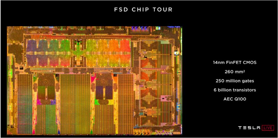
Figure: Tesla Full Self-Driving Architecture Display
As we approach 2020, we see automotive ASIC manufacturers addressing this challenge by developing new ASIC architectures that include embedded FPGA (eFPGA) semiconductor intellectual property (IP). Although eFPGA was not mainstream technology when Tesla developed its full self-driving chip in 2016, it has now become mainstream technology. Achronix eFPGA IP is now in production in multiple high-volume applications, proving that Achronix has the capability to achieve mainstream production. Now, we see eFPGA IP being adopted by automotive OEMs to embed hardware programmability to tackle the aforementioned new challenges.
Unlike standalone FPGA chips that only offer specific logic densities, memory, resource combinations, and I/O interfaces, eFPGA IP solutions can be fully customized for specific automotive workloads.Compared to standalone FPGAs, eFPGA can save up to 90% in costs and reduce power consumption by up to 75%, while still providing the same capability to add new hardware features after the ASIC is developed. For example, changing hardware specifications to provide enhanced radar and camera sensor fusion to meet the demands of innovative functionalities, new and more powerful display technologies, and new image sensor capabilities. The block diagram below shows some functionalities that an integrated eFPGA ASIC can provide to automotive manufacturers.
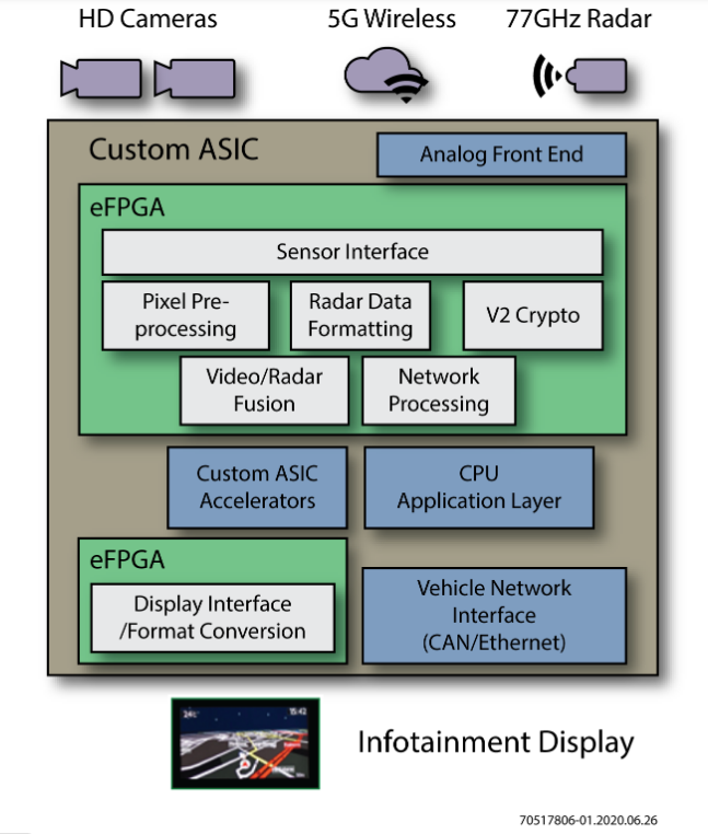
HD Cameras: HD Cameras
5G Wireless: 5G Wireless
77GHz Radar: 77GHz Radar
Custom ASIC: Custom ASIC
Analog Front End: Analog Front End
eFPGA: Embedded Field Programmable Gate Array
Sensor Interface: Sensor Interface
Pixel Pre-processing: Pixel Pre-processing
Radar Data Formatting: Radar Data Formatting
V2 Crypto: V2 Crypto
Video/Radar Fusion: Video/Radar Fusion
Network Processing: Network Processing
Custom ASIC Accelerators: Custom ASIC Accelerators
CPU Application Layer: CPU Application Layer
Display Interface/Format Conversion: Display Interface/Format Conversion
Vehicle Network Interface (CAN/Ethernet): Vehicle Network Interface (CAN/Ethernet)
Using Achronix‘s Speedcore eFPGA IP technology can achieve this architecture. Speedcore eFPGA IP provides a competitive advantage over traditional ASICs by helping manufacturers shorten development time while allowing for the addition of entirely new and innovative functionalities that can be defined after the ASIC hardware architecture is finalized.eFPGA IP is truly a game-changer for the automotive industry.Achronix is excited to see how eFPGA can bring tremendous value to future automotive ASIC designs. You can email [email protected] to contact us now for more information about our automotive solutions.