This article is approximately 6000 words long, with a recommended reading time of 15 minutes. Please follow the New Fortune WeChat account.
Independent innovation is not about working behind closed doors, but about maintaining the controllability of core technologies through open cooperation.
The rise of the industry does not require blind adherence to cutting-edge technologies, but rather achieving irreplaceability in niche areas.
Focusing on specialized process foundry and deeply cultivating power semiconductors strategically avoids the technical barriers of advanced processes in the short term, while long-term reliance on the demand of China’s new energy industry chain forms an industry moat. This, in turn, promotes industrial technology synergy through capital integration and solves domestic market dilemmas with specialized processes.
 01
01
The Starting Point of National Strategy
In the 1990s, the export of semiconductor technology from overseas to China followed the rules of the Wassenaar Arrangement, which basically approved exports according to the “N-2” principle (i.e., technology exports must be at least two generations behind). Therefore, starting in 1996, the country invested heavily in the “909 Project” to create independently controllable semiconductor manufacturing technology.
Shanghai Huahong Microelectronics was established as the main engineering entity, with the first chairman, Hu Qili (former Minister of the Ministry of Electronics Industry of China), personally leading the project. The registered capital was 4 billion yuan, with the central government and Shanghai’s finances contributing in a 6:4 ratio, mainly used for building chip production lines. The total investment in the project exceeded 10 billion yuan, shouldering the historical mission of China’s semiconductor industry’s autonomy.
In 1997, Huahong Group, responsible for the “909 Project,” began construction in Shanghai. At that time, the domestic semiconductor industry had just experienced two painful defeats—the Shaoxing “907 Project” and the Wuxi “908 Project,” especially the painful lessons from the “908 Project” (Wuxi Huajing Project): nearly ten years of delays (in approvals and equipment imports), closed-door manufacturing technology, and a manufacturing technology gap that expanded to more than two generations, leading to continuous losses. The industrial planning route at that time not only wasted precious time for technological catch-up but also exposed the limitations of independent research and development and the fatal weakness of being disconnected from the global market’s commercialization progress.
Faced with this dilemma, the “909 Project” urgently needed a new path—it had to avoid repeating past mistakes and shift from “closed-door manufacturing” to “learning from past experiences.” Against this backdrop, Huahong made a strategic choice: to engage in deep joint ventures with NEC Corporation, the second-largest semiconductor company in the world at the time, establishing Huahong NEC. This decision not only marked the transformation of China’s semiconductor industry from “self-reliance” to “borrowing a boat to go to sea” but also ensured the rapid advancement and commercial success of the “909 Project” through NEC’s technology, orders, and management experience, laying the foundation for the rise of China’s semiconductor industry and initiating a model of industrial breakthrough in China by “exchanging capital for time.”
As a giant in the global semiconductor industry at that time, NEC’s status and influence provided Huahong with indispensable strategic support. NEC was once the largest semiconductor company in the world (surpassed by Intel in 1992), and its participation in the construction of China’s semiconductor industry was not accidental: its chairman, Kanemoto Nobuhiko, had far-reaching strategic vision and actively sought cooperation based on NEC’s long-term interests in the Chinese market, offering negotiation conditions far exceeding domestic expectations. Specifically, NEC not only invested $200 million in cash (holding nearly 30% of the shares) but also committed to transferring 0.5 to 0.35-micron process technology (then the mainstream international level) and guaranteed full-load operation of the production line—products for domestic use would be sold back to the international market by NEC. Further industrial analysis shows that the scale of investment in chip production lines is enormous, and the largest part of the product’s cost structure is usually equipment depreciation; thus, ensuring capacity utilization is largely a guarantee of profitability. Meanwhile, Huahong held 70% of the shares, ensuring control, while the Japanese side also took on management and technical training, forming a forward-looking cooperation framework of “long-term cooperation, priority on benefits.”
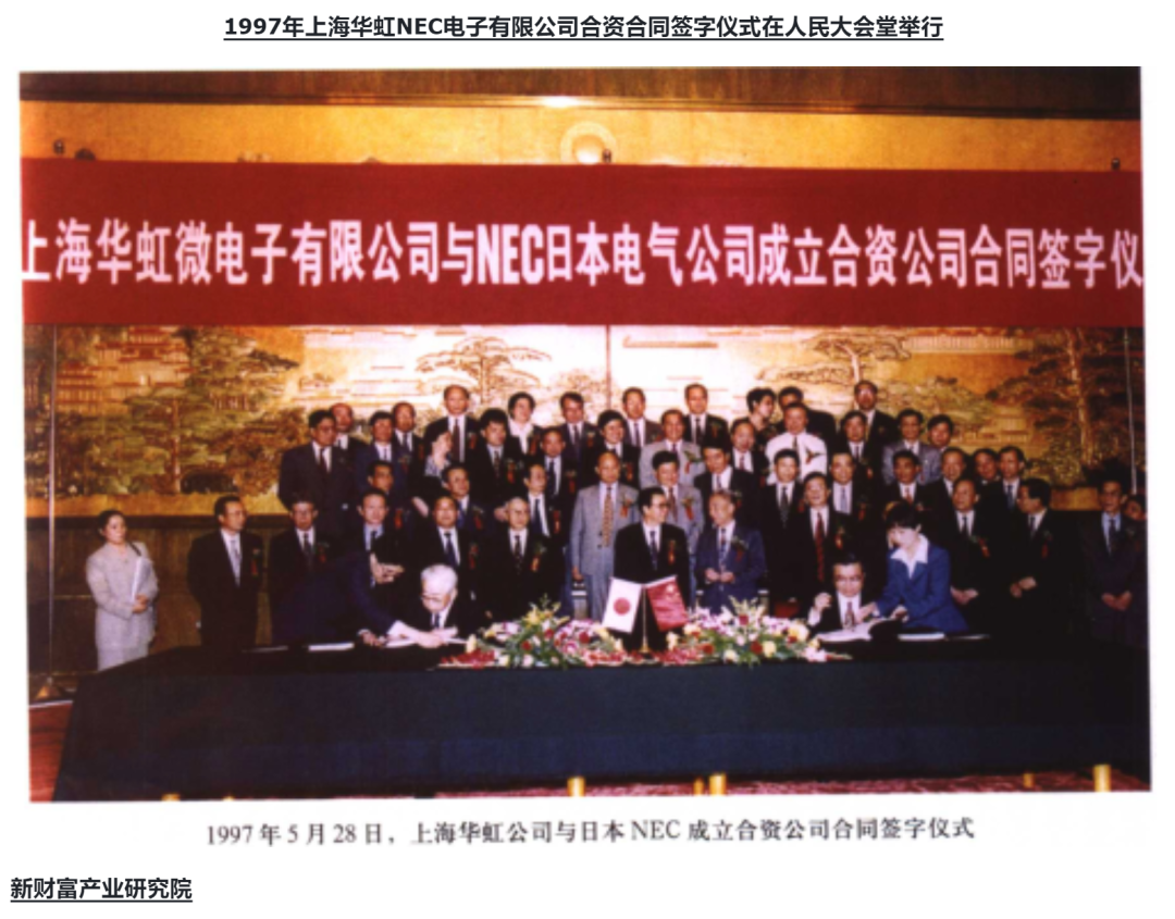
Looking back now, this top-level strategic design largely targeted the root causes of the previous “908 Project” failure, and by gradually introducing foreign capital, Huahong avoided the risks of falling behind in technological progress and lacking market demand, positioning its main products in the highly demanded 64MB DRAM, precisely aligning with the global supply chain. This joint venture model proved to be remarkably efficient compared to the prolonged delays of the “908 Project”: construction began in July 1997, and mass production was achieved in February 1999, taking just over a year to successfully produce China’s first 64MB DRAM chip; by 2000, sales reached 3 billion yuan, with a net profit of 500 million yuan, simultaneously achieving export earnings. From then on, China’s semiconductor industry began to achieve dual breakthroughs in both commercial and technological aspects. Overall, this success was by no means accidental; it stemmed from a complete abandonment of “domestic closed-door manufacturing”: NEC’s order guarantees (products covering mainstream 64MB DRAM, domestic IC bus card chips, etc.) ensured capacity utilization, while NEC’s technology transfer, domestic employee training, and management of the enterprise significantly accelerated the improvement of profitability in the domestic semiconductor industry at that time.
Entering the 21st century, with the global DRAM price war (the impact of Korean companies) and NEC’s international status significantly declining, the semiconductor industry’s 18-month generational Moore’s Law also put pressure on Huahong to transform. Nevertheless, Huahong’s joint venture with NEC achieved a miraculous industry milestone at a critical historical juncture: it not only avoided the pitfalls of the “908 Project” but also successfully integrated into the global semiconductor industry chain in a shorter development time. This strategy remains an important lesson for the internationalization of China’s high-tech industry.
02
Creating “Irreplaceability” in Mature Processes
In 2003, after experiencing the global DRAM price war, Huahong Group decisively adjusted its strategy, reclaiming operational control and gradually halting DRAM production, fully transitioning to the wafer foundry sector. This transformation was not only a survival choice but also a preliminary practice of China’s semiconductor industry’s autonomy: by focusing on urgently needed chips in the domestic market, which had lower design difficulty and could reflect national will, Huahong positioned IC card chips, communication chips, and power devices as its strategic development direction.
From then on, Huahong broke through the international monopoly with technological advancements—achieving breakthroughs in embedded non-volatile memory in 2001, independently developing IC card chips, and ending the complete reliance of the domestic IC card market on overseas imports. In 2004, as the domestic layout for the second-generation ID card began, Huahong became the largest supplier of ID card IC chips, providing over 75% of the IC chips nationwide and over 80% of the social security card IC chips, saving the country over 100 billion yuan in chip import costs, thus establishing its market position as the world’s largest IC card chip foundry, which also provided crucial support for its business transformation and early cash flow accumulation. Meanwhile, in addition to the government orders for IC card chips, Huahong also needed highly market-oriented products to compete in the global market. At that time, China had just joined the World Trade Organization, and the domestic demand for power devices surged, prompting Huahong to enter the power semiconductor market and gradually grow into the world’s leading power device foundry through the synergy of 8-inch and 12-inch production lines, providing core support for strategic assets such as new energy vehicles and photovoltaics in China.
Further industrial analysis shows that the deeper significance of this transformation lies in: it is not only a switch in business models but also a reconstruction of technological routes. Huahong timely abandoned the “arms race” of pursuing advanced processes, instead deeply cultivating differentiated specialty processes (embedded/standalone non-volatile storage, power devices, analog and power management, logic and RF), thereby creating “irreplaceability” in mature processes. By 2025, Huahong Semiconductor led the global specialty process foundry with a quarterly capacity utilization rate of 102.7% in Q1, while the full production state of the production line largely highlighted its scarce value in the mature process field. Overall, Huahong’s transformation journey is a microcosm of China’s semiconductor industry transitioning from technological dependence to industrial autonomy, providing a path for future practitioners to “avoid the red sea and forge long boards” for corporate survival.
In 2005, Huahong NEC was restructured into Huahong Semiconductor, marking a new starting point from “joint venture technology introduction” to “independent capital operation”—this move not only avoided the risk of terminating technical cooperation with NEC but also paved the way for subsequent international financing. Subsequently, Huahong Semiconductor was registered in Hong Kong, marking a key step in capitalizing the main body of the “909 Project”—Huahong Semiconductor was not a newly established entity but served as the holding parent company of Huahong NEC, aiming to restructure the equity structure to connect with international capital markets. This layout continued to achieve another breakthrough in 2011: Huahong Semiconductor completed a merger with Grace Cayman (the parent company of Shanghai Hongli Semiconductor), integrating Huahong’s power device technology accumulation with Hongli Semiconductor’s flash memory process advantages, and officially established Shanghai Huahong Hongli Semiconductor Manufacturing Co., Ltd. in 2013 (most of Huahong Semiconductor’s related business is conducted through this subsidiary), beginning the deep integration of technology platforms and capacity resources.
In 2014, it became a highlight in the development history of Huahong Semiconductor, as its listing on the Hong Kong main board not only injected capital vitality but also confirmed the commercial value of the specialty process route—by then, Huahong’s cumulative shipments of power devices had exceeded 2 million wafers, with high-end products such as super junction MOSFETs and IGBTs continuously increasing in the industrial and new energy sectors. Behind this achievement is actually a result of twenty years of technological cultivation: Huahong began mass production of the MOSFET process platform in 2002; in 2007, it broke through the 0.35μm BCD process for producing analog and power management chips; in 2014, the high-margin SIM card chip shipments reached nearly 3 billion pieces, capturing over 50% of the global market share, providing cash flow for eFlash research and development, and promoting the pre-research of 55nm processes; in 2016, 90nm embedded flash memory eFlash was successfully mass-produced.
03
The “Strongest Business Line” of Power Semiconductors
In 2018, amid the global wafer shortage crisis, coinciding with the beginning of the semiconductor industry’s upward cycle, Huahong Semiconductor began its 12-inch capacity expansion strategy. In January 2018, the Wuxi municipal government, the National Big Fund, and Huahong Semiconductor jointly invested to establish Huahong Semiconductor (Wuxi) Co., Ltd., launching the first phase of the Wuxi project (Huahong Plant 7), with a total investment of up to $10 billion for three phases, with the first phase investment of about $2.5 billion. This project was completed and put into production in September 2019, taking only 533 days, setting a record for Huahong’s fastest production, and becoming the world’s first 12-inch power device production line, with a planned monthly capacity of at least 70,000 wafers. From then on, Huahong began a leapfrog development from 8-inch processes to 12-inch, leveraging the platform advantages of 8-inch in 0.35 microns to 90 nanometers and 12-inch in 90 nanometers to 55 nanometers.
The 12-inch production line will be a key driver for Huahong’s long-term revenue and profit growth, especially as Huahong Wuxi utilizes the mature technology of the existing 8-inch production line to rapidly introduce power devices, non-volatile storage, analog and power management, and other specialty process platform product lines into the 12-inch production line, while also adding CIS, NOR Flash, and other product lines, thus laying the strategic foundation of “8+12 inches.” This strategic upgrade significantly optimized Huahong’s capacity structure within three years—between 2019 and 2022, the revenue share of 8-inch decreased from 98% to 60%, while the revenue from 12-inch surged from less than 1% to 40%.
From then on, Huahong began to focus on specialty processes rather than competing based on Moore’s Law—by 2021, Huahong and SIDA Semiconductor achieved large-scale production of automotive-grade IGBT chips and 12-inch IGBTs, with its self-developed second-generation chips (equivalent to the international sixth-generation FS-Trench chips) successfully breaking the monopoly of international giants on 3300V and above high-voltage IGBT chips. Huahong also became the world’s first pure foundry company to mass-produce automotive-grade IGBTs on both 8-inch and 12-inch production lines; in 2022, it further launched 55nm high-speed MCU embedded flash memory and 12-inch automotive-grade super junction MOSFETs. The layout of these core technologies not only improved Huahong’s product gross margin but also further solidified its market position as the second-largest wafer foundry in mainland China.
SIDA Semiconductor, as one of the only two domestic power semiconductor companies ranked among the top ten in the global IGBT module market share, is also the core supplier that has penetrated the most mainstream vehicle manufacturers in China. The strategic cooperation with SIDA essentially represents a collaboration between the Fabless model (SIDA’s design) and foundry manufacturing (Huahong’s production). Currently, multiple voltage series from 650V to 3300V and above have achieved mass production and terminal acceptance. Huahong, leveraging nearly twenty years of research and development in power devices, has successfully introduced the stringent requirements for automotive-grade IGBTs—high current, low loss, and high reliability—into the 12-inch production line, successfully narrowing the technology gap (Infineon has already mass-produced seventh-generation IGBT chips and completed the eighth-generation research and development) to about one generation (3-5 years).
Overall, wafer foundry presents two paths: following the micro-fine competition of Moore’s Law or developing specialty processes along Moore’s Law. Clearly, Huahong chose the latter—achieving global irreplaceability at the 55nm/90nm nodes.
In 2023, amid the overall pressure on the global wafer foundry market, Huahong’s power device business demonstrated strong resilience, becoming the most prominent growth driver in its revenue structure. Huahong’s revenue in 2023 decreased by 7.7% year-on-year to $2.286 billion, but the power device segment achieved sales revenue of $902 million, a year-on-year increase of 16.5%, accounting for nearly 40% of revenue, significantly surpassing the 30% revenue share of embedded storage, making it Huahong’s largest revenue source. Further industrial analysis shows that this achievement largely highlights Huahong’s strategic foresight in the specialty process field—as the only company globally with both 8-inch and 12-inch power device foundry capabilities, its breakthroughs in core technologies such as super junction MOSFETs and IGBTs are evident. Moreover, power semiconductors, as the core of automotive electronics, are the second-largest core component in new energy vehicles, next to batteries. The upcoming demand and product iteration for IGBTs, MOSFETs, and other power devices in new energy vehicles and charging piles will usher in a significant transformation not seen in a century.
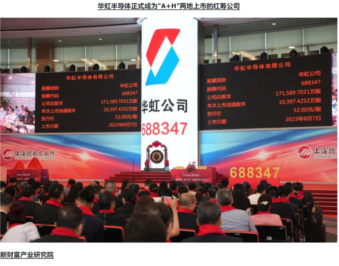
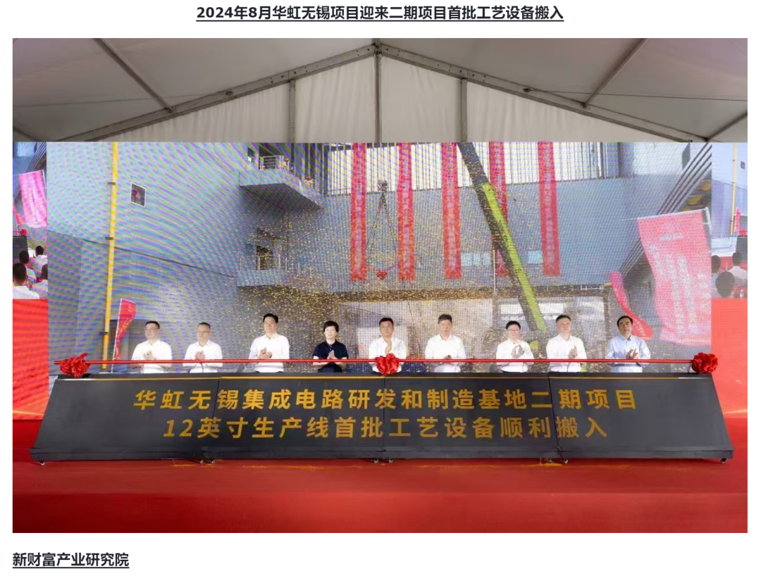
It is worth noting that after the first phase of the Wuxi project was put into production, Huahong immediately launched a new round of development planning, also using the Sci-Tech Innovation Board listing as a lever—being the largest IPO in A-shares at the time, Huahong successfully raised over 20 billion yuan, which not only demonstrated investors’ confidence in leading Chinese semiconductor companies but also directly accelerated the subsequent nearly $7 billion investment in the second phase of the Wuxi project (Huahong Plant 9). This second phase project focuses on automotive-grade chip manufacturing, with a planned monthly capacity of at least 80,000 12-inch wafers, covering advanced specialty processes and high-end power semiconductors from 65/55nm to 40nm. Notably, this project was constructed in just over a year: officially starting in June 2023, the first batch of equipment is scheduled to be moved in by August 2024, and mass production is expected to be achieved by December 2024, with construction progress comparable to that of the first phase project.
Looking back now, the breakthrough of this second-phase production line has profound significance for China’s semiconductor industry chain: first, after the full production of both phases in Wuxi, the combined monthly capacity will reach at least 180,000 wafers, becoming the world’s largest 12-inch power semiconductor device foundry platform; second, relying on the accumulation of automotive-grade processes, the second phase project strengthens the technical extension of high-end power devices, directly targeting the domestic chip demand for new energy vehicles and industrial control. By 2025, as a key node for the ramp-up of the second phase capacity, Huahong Plant 9 is expected to gradually release capacity to 30,000 wafers/month, ultimately aiming for 80,000 wafers. Overall, Huahong is constructing a multi-dimensional process foundry with leading barriers globally through the “8-inch + 12-inch” collaborative expansion and the “specialty process + power devices” dual-track strategy.
In 2024, driven by the weak recovery of the semiconductor industry, Huahong presented a revenue pattern of “increased volume and reduced price.” The annual revenue is expected to be around $2 billion, a year-on-year decrease of 12%, mainly due to the high pressure of previous inventory and the drag of weak recovery. However, the improving momentum in the second half of the year still highlights the resilience of the domestic market, with downstream application areas such as consumer electronics and the automotive industry generally leading the global pace in inventory digestion. Specifically, the annual capacity utilization rate is close to 100%, with the equivalent 8-inch wafer shipment volume increasing by over 10% year-on-year, but the decline in ASP and the depreciation pressure of new production lines significantly impacted the gross margin, which only reached 10% for the year, with net profit plummeting by 80% year-on-year, largely exposing the structural challenges of product revenue—this performance foreshadows the “K-shaped recovery” of the global semiconductor market: demand for consumer electronics (image sensors, power management chips, logic and RF) has begun to open an upward cycle, thus boosting Huahong’s revenue growth by 19% year-on-year in Q4 2024. In contrast, the cyclical turning point for the automotive industry is roughly four quarters behind that of consumer electronics—therefore, Huahong’s power devices must navigate the short-term depreciation pressure and long-term technological layout while also addressing the mismatch between the recovery of consumer electronics and the lagging demand from the automotive industry. Huahong Semiconductor must persist through the trough and gather strength to climb the next growth peak.
04
Conclusion
Huahong Semiconductor’s thirty years represent a profound epic of China’s will and market-driven rise. Looking back, its rise began with the strong drive of national strategy, rooted in the “909 Project”—this project, as the largest semiconductor project in the history of China’s electronics industry at that time, involved total investments exceeding 10 billion yuan, personally promoted by senior officials of the central government, thus determining the country’s determination to “spend everything to make it happen.” During this stage, Huahong transitioned from DRAM production to wafer foundry, completing the preliminary transformation from technology introduction to independent innovation, laying the groundwork for the subsequent market-driven rise centered on power semiconductors.
Entering the market-oriented phase, Huahong cracked the domestic market dilemma with differentiated specialty processes. Faced with the “arms race” of advanced processes and the equipment blockade by international giants, Huahong avoided the technological iteration risks of high-end processes below 14nm, instead deeply cultivating specialty processes above 55nm, thus constructing an industry moat centered on “specialty processes + power devices.” Currently, its five major specialty process platforms (embedded/standalone non-volatile storage, power devices, analog and power management, logic and RF) cover multi-dimensional application areas such as new energy vehicles, industrial control, and consumer electronics. With cost advantages, process stability, and high reliability, Huahong ranks first in global power device foundry capacity, and is expected to break into the top five global pure foundry companies by 2026-2027, achieving a significant leap in industrial status.
Currently, the global semiconductor industry is facing an unprecedented transformation, and Huahong still needs to seek a balance in its development strategy amid material innovation (third-generation semiconductors), capacity utilization (ramping up Wuxi phase two), and international blockades (restrictions from the Wassenaar Arrangement). However, Huahong has proven that the rise of China’s chip industry does not require blind adherence to cutting-edge technologies, but rather achieving irreplaceability in niche areas, thus opening a sustainable path for the rise of China’s semiconductor industry.
– END –
Any information and insights mentioned in this article are solely the author’s personal opinions or statements regarding specific events and do not constitute recommendations or investment advice. Investors should bear the risks and consequences arising from investments made based on this information.