Question 1: How is the code in FLASH executed? For example, where is the PC pointer set and by whom?
Taking ARM as an example:
Microcontrollers such as ARM Cortex-M3/4 (like STM32, etc.): The code for this type of microcontroller runs directly in NOR flash, and the Cortex core can execute it directly without needing to load it into RAM.
ARM Cortex-A series SoCs (like Exynos4412): This type of SoC is more complex, usually has a memory management unit (MMU), and the code is stored in NAND flash. During execution, the code needs to be loaded into RAM; the boot process of this type of SoC includes loading the program. Just like how the Windows operating system is stored on a hard drive, when booting, the operating system’s code is loaded into RAM.
PC Pointer: Regardless of the microcontroller or SoC, there is a PC register that holds the address of the next instruction to be fetched. Normally, it increments by “4”; when a branch is encountered, the value is set by the jump instruction. So what is a pointer? A pointer is the address of a variable. In systems with an operating system (like Linux or Windows) that includes a memory management unit (MMU), the pointer is a virtual address. Without an operating system, it is a physical address, and the MMU translates between virtual and physical addresses.
Question 2: Do these codes need to be moved to RAM to execute? What happens if this is not done?
As mentioned above, most microcontroller codes run directly in NOR flash, while a few need to be loaded into RAM. NOR flash can address a byte directly, allowing specific instruction addresses to be found, thus enabling direct execution. NAND flash stores data in blocks, meaning instructions cannot be directly addressed, so programs stored in NAND flash cannot execute unless loaded into RAM. This is akin to your Windows operating system not running if it is not loaded into RAM.
Question 3: If it needs to be moved to RAM, is there a difference between on-chip and off-chip?
Both on-chip and off-chip can be used; it depends on the specific SoC or CPU.
Question 4: If the actual code size in FLASH (e.g., 1MB) exceeds the available space in RAM (e.g., 512KB), what does the transfer process look like?
Such situations are rare. However, there may be systems with small RAM, which can use time-slicing or segment loading, meaning run one segment, load another, finish running, and load the next segment. This is not recommended as current RAM sizes are large; when your actual code reaches 1MB, your memory could be 1GB or 2GB. For instance, after compiling, a Linux operating system only needs a few MB, while the actual Linux system can have several GB of available memory.
Question 5: What are the performance speed differences between off-chip FLASH and SRAM compared to on-chip?
The specifics depend on the SoC’s bus design. Generally, off-chip performance tends to be weaker.
Whether a program can run directly in Flash depends on the access characteristics of the Flash.
Flash memory is organized in blocks, and using it is more efficient when accessed in blocks. Flash is similar to ROM-type storage but is actually read-write. Unlike RAM, which can write data easily, Flash requires the block containing the data to be erased before writing. Therefore, to rewrite data in Flash, the block is first cached in memory, modified, and then written back to ensure data is not lost, though this is costly. During read operations, the block’s location is usually identified first, and data is read sequentially within the block. Random reading between different blocks is very inefficient, so reading and writing in blocks is a significant characteristic of Flash; it cannot address storage areas arbitrarily, as seen in typical NAND Flash.
However, a specific type of Flash memory allows arbitrary addressing during read operations without significant costs; its read operation is close to that of RAM, while the write operation still follows the block erase and block write characteristic, typical of NOR Flash.
Thus, due to these characteristics, Flash is typically used for storing non-frequently modified data that must not be lost during power outages.
After explaining the background knowledge, let’s return to the questions:
First, it is essential to understand that the CPU needs to read instructions from memory, and the instruction address is provided by the PC register. After executing an instruction, the PC automatically points to the next instruction. If the instruction lengths vary, the provided addresses may not always align consistently. Furthermore, program execution always involves jumps, making instruction addressing more arbitrary. Therefore, to execute a program directly in a specific type of memory, at least the ability to read data must allow arbitrary addressing, and NOR Flash meets this requirement. The commonly found Flash in MCUs is of this type, allowing programs stored on it to run directly without needing to load into RAM. Other types of memory that do not possess this access feature cannot execute programs directly and must be transferred to suitable memory types to execute, such as loading into RAM.
1. How is the code in FLASH executed? For example, where is the PC pointer set and by whom?
Microcontrollers using Cortex-M cores will map the startup memory to the address 0x00000000 based on the level of external startup configuration pins. If it starts from Flash, an exception interrupt vector table is stored at the beginning of the internal Flash, with the first two entries containing the initial stack address and reset vector. The position of this table is configurable, and after reset, the position is at 0x00000000. After powering up and resetting, the SP and PC registers are automatically set to the first two entries of the table, and execution begins based on the initial value set by the PC.
2. Do these codes need to be moved to RAM to execute? What happens if this is not done?
As previously described, it is not necessary. Executing in RAM may yield better performance, but for internal MCU Nor Flash, it is not required. It is worth mentioning that programs generally consist of a code section (txt), a read-only data section (rodata), an initialized data section (data), and an uninitialized data section (bss, which has no data). The read-only data section, like the code section, does not need to change, so it can remain in Flash. However, the data section stored in Flash must be loaded into RAM, freeing up space for bss. This is part of the environment initialization process, which involves moving data, not code, occurring before entering the main function.
3. If it needs to be moved to RAM, is there a difference between on-chip and off-chip?
On-chip RAM generally performs better, but its capacity is usually limited.
4. If the actual code size in FLASH (e.g., 1MB) exceeds the available space in RAM (e.g., 512KB), what does the transfer process look like?
It can be loaded in stages for execution, but program organization becomes complex, and execution becomes inefficient. If this occurs, consider upgrading hardware or optimizing the program.
5. What are the performance speed differences between off-chip FLASH and SRAM compared to on-chip?
This depends on the clock rate and access latency of the memory. Generally, integrated internal memory performs better than off-chip memory, so to achieve higher execution performance, internal memory should be prioritized. In low-end MCUs, due to low operating speeds, there may not be significant differences between internal and external memory.
This question can be answered from three perspectives:
1. Principles of computer organization
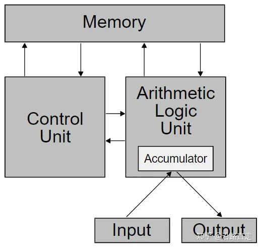
Students in computer science must be familiar with this classic computer model. All computing devices (including embedded systems) adhere to this model. The five components can be divided into three parts: (1) CU and ALU are the CPU (2) Memory is the memory device (ideal memory device) (3) Input and Output are various peripheral devices (keyboard, mouse, monitor, etc.).
Our focus here is on the memory device. In the Von Neumann model, Memory is imagined as an ideal memory device. An ideal memory device is one that is read-write, non-volatile, and allows random read/write access. For theoretical models, simplicity and clarity are key. However, in reality, it is not so ideal due to cost constraints, and different types of memory can only satisfy some of these criteria, which leads to the mainstream memory types discussed next.
2. Characteristics of mainstream memory
Current memory can be broadly classified into two categories: RAM and ROM. Many summaries exist regarding the specific definitions and development history of these two types of memory, so I will not elaborate further. Instead, I will share my personal understanding of these two types of memory.
(1) RAM, which can be further divided into SRAM and DRAM
Common characteristics (the fundamental characteristics of RAM): Read-write, random read/write
Differences: SRAM is ready to use when powered, while DRAM requires initialization before use, and the cost per unit of SRAM is higher than that of DRAM.
(2) ROM, which can be divided into hard drives and Flash (NOR Flash and NAND Flash)
Common characteristics: Non-volatile
Differences: Both hard drives and NAND Flash require block-level read/write access, while NOR Flash allows random reads but requires block writes.
The non-volatile and random read characteristics of NOR Flash make it suitable as a system boot medium.
3. The speed difference between CPUs and memory is a major factor limiting computer performance today.
4. Specific answers to the five questions above
(1) It depends on the type of Flash. If it is NOR Flash, the system can access and execute it directly. If it is NAND Flash, the code needs to be loaded into RAM to run. The PC register is in the CPU and is set to a specific value (e.g., the default for ARM Cortex-M3 is 0x4) when powered on.
(2) As in the first question, whether the code needs to be moved depends on the type of Flash.
(3) If the RAM types are the same, there is no difference between on-chip and off-chip. If the RAM types differ, a specific analysis is needed.
(4) Assuming the Flash is 1MB and RAM is 512KB, it is likely that this is NOR Flash and SRAM (e.g., STM32), so the code does not need to be moved. If it is NAND Flash, it will generally be paired with DRAM, which will have a much larger capacity, so this assumption may not hold.
Regularly share embedded knowledge in an easy-to-understand manner,follow our public account, mark it as a favorite, and improve a little every day.
Disclaimer:
All articles and images published by this account are owned by the original authors. If there is any infringement, please contact us for removal.
 Follow, like, view, and share to support quality content!