NVIDIA has invested a significant amount of resources in the field of artificial intelligence, as AI is widely regarded as the next potential trillion-dollar market. In the second half of 2018, NVIDIA released the new Xavier processor, followed by the Jetson AGX computing platform based on the Xavier processor. As a product designed for markets such as artificial intelligence, robotics, and autonomous driving, what unique internal designs and architectures do the Xavier processor and Jetson AGX have? Today, this article will explore these details with you.
NVIDIA has not been aggressive in processor development, especially in general-purpose processors. Since the Tegra exited the mobile platform, apart from some special devices, the main use of Tegra has been in artificial intelligence platforms. NVIDIA has invested heavily in the AI market, especially standing out in deep learning. To further enhance its influence in AI, robotics, and autonomous driving, NVIDIA released the new Xavier processor in August 2018, and in early 2019 launched the Jetson AGX platform, hoping to deliver stronger performance and a better application experience for related applications and markets. What kind of powerful performance can the Xavier processor, developed by NVIDIA specifically for AI-related platforms, bring?
NVIDIA has accumulated a certain amount of experience in processor development, with the Tegra series processors for mobile devices initially being well-received in the market. However, the Tegra processor has not been updated for several years, and NVIDIA has launched a new brand, Xavier, in the AI-related industry. From the brand layout, it seems that Tegra no longer targets the B2B market, and Xavier is the main product in this market.
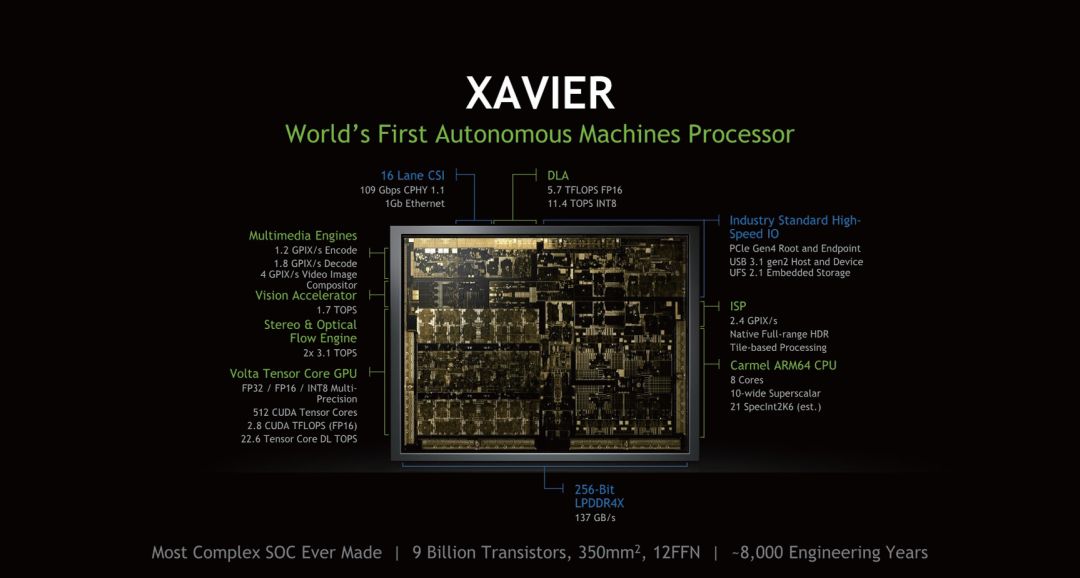
Xavier is the largest SoC chip that NVIDIA has released to date. It contains 9 billion transistors, is manufactured using TSMC’s 12nm process, and has a chip area of 350 square millimeters. What does 350 square millimeters mean? To put it in perspective, the GP102, known as a large core, has a core area of only 471 square millimeters, while the lower-end GP104 core area is only 310 square millimeters. Therefore, considering various factors such as transistor count and chip area, Xavier can be considered a giant among ARM SoCs.
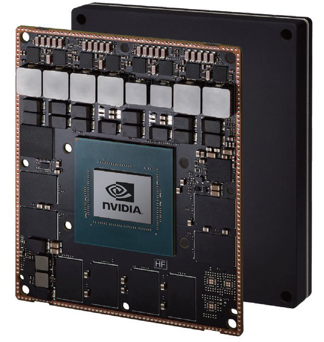
▲Front photo of the Xavier chip
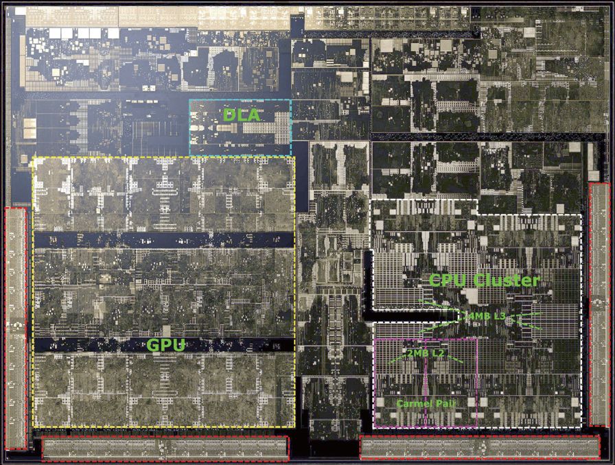
The large chip area indicates that the expected performance metrics are also very high. This can be inferred from the architectural layout of Xavier. The internal structure of Xavier mainly consists of two large parts: one part is an 8-core Carmel architecture CPU, and the other part is a Volta architecture GPU.
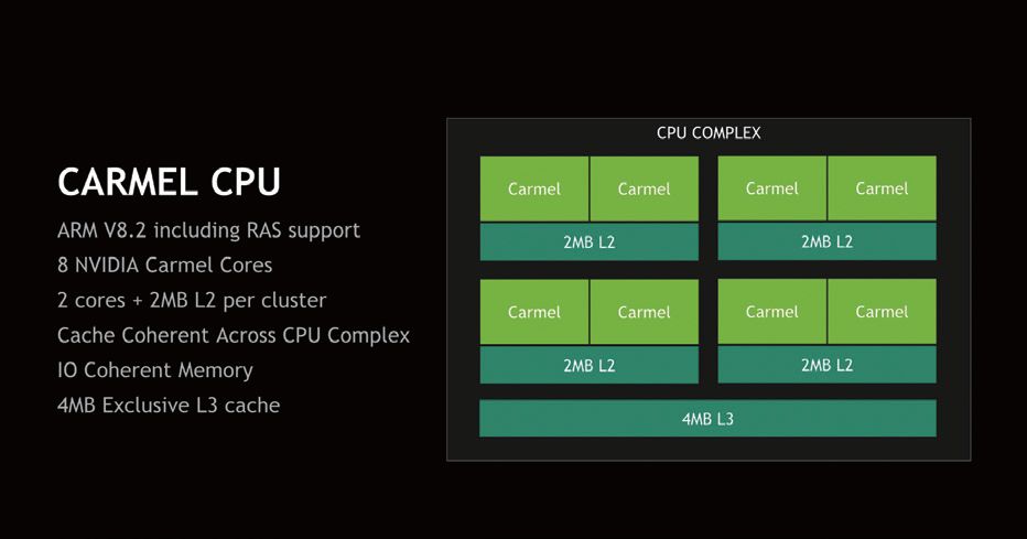
On the CPU side, the 8 Carmel cores are divided into 4 clusters, with each cluster containing a set of Carmel CPUs, each controlled by an independent clock unit, and the 2 CPUs within each cluster share a 2MB cache. The CPU portion of Xavier shares a 4MB L3 cache among the 4 clusters. Currently, NVIDIA has not provided any detailed information about the Carmel architecture, only vaguely referring to it as a 10-wide superscalar architecture, which is almost identical to the previous Denver architecture. Additionally, the Carmel architecture supports the ARMv8.2 instruction set, including support for RAS instruction sets.
▲Xavier chip with multiple features
▲Xavier uses NVIDIA’s self-developed Carmel CPU
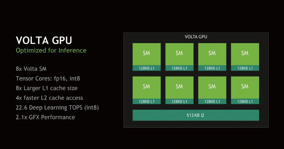
On the GPU side, Xavier includes 4 TPCs from the Volta architecture, with each TPC containing 2 SMs, totaling 8 SMs that include 512 CUDA Cores or ALU channels. The GPU section of Xavier not only includes the traditional CUDA Core part but also incorporates Tensor cores from the Volta architecture, enabling it to perform deep learning computations. The Tensor cores in Xavier can execute FP16 or INT8 tensor calculations, achieving a performance of 22.6 DL TOPS under INT8 or 11.3 FP16 TOPS. Additionally, the CUDA cores can perform FP16 and FP32 calculations at 2.8 TFLOPS and 1.4 TFLOPS, respectively.
▲The GPU used in Xavier comes from the desktop Volta architecture
▲Different parts of the Xavier chip
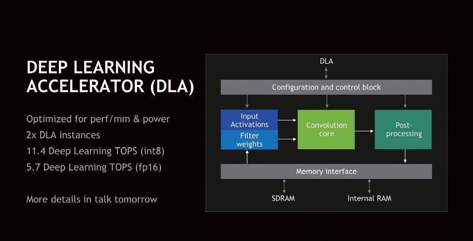
In addition to the CPU and GPU, NVIDIA has also designed a DLA module for Xavier, which is a deep learning acceleration module containing 2 DLA cores. This module is primarily focused on accelerating deep learning computations, similar to the AI cores paired with Huawei’s HiSilicon processors or Apple’s A12. NVIDIA claims this module has outstanding performance-to-power ratio in deep learning computations. The DLA performance is 11.4 DL TOPS under INT8 or 5.7 DL TOPS under FP16.
▲Xavier enhances deep learning capabilities
As computer vision capabilities become increasingly important, Xavier has also added a PVA vector processing unit, which is a programmable vision accelerator. This module focuses on vision-related processing and can handle basic tasks in object detection faster and better than the GPU or DLA module. Each PVA vector processing unit is designed to execute 7-wide VLIW architectures at a time, consisting of 2 scalar, 2 vector, and 3 memory instructions. Each cycle, the PVA can perform 8 32-bit, 16 16-bit, or 32 8-bit mathematical operations.
NVIDIA designed 2 PVA modules, each containing a Cortex-R5 core for control and configuration, 2 vector processing units, and 2 DMA units dedicated to data management. The PVA has its own instruction cache and data storage unit, allowing for independent operation.
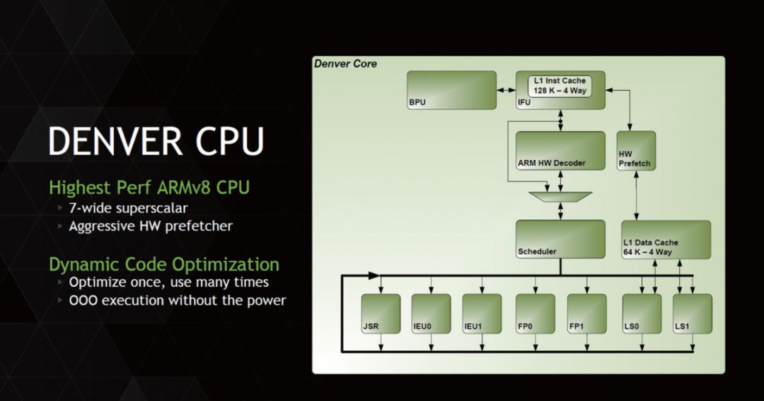
The CPU portion of the Xavier processor is codenamed Carmel and adopts a completely different design approach from other ARM processors currently on the market. Although NVIDIA has not disclosed detailed information about Carmel, some promotional language reveals the inheritance relationship between Carmel and the Denver architecture.
Speaking of the Denver architecture, users familiar with NVIDIA’s processor development history should have some impressions. This mysterious architecture was announced in 2011 with the Project Denver plan. Project Denver was a special R&D program aimed at high-performance mobile devices or other scenarios requiring certain performance standards, with NVIDIA investing hundreds of top processor engineers in its development.
▲The Denver architecture can be said to mark NVIDIA’s first attempt at self-developing CPU architecture
After years of effort, in 2014, the final product of Project Denver was the Denver architecture processor, which was applied to the Tegra K1 processor specifically for Google’s Nexus 9 version. This processor did not enter the mobile market, and its mobile products are extremely rare, with the Nexus 9 being possibly the only product readily available in the market.
NVIDIA claims that the Denver architecture is the first 7-wide superscalar processor architecture. Among Denver’s contemporaneous products, the Cortex-A15 adopts 3-issue, the Cortex-A12 adopts 2-issue, and even the Cortex-A73, years later, only uses 2-issue products, with only the latest Cortex-A76 adopting 4-issue to expand front-end decoding capabilities. Therefore, the so-called 7-issue solution of the Denver architecture is quite thought-provoking, as it far exceeds the level of processors in the same class at that time.
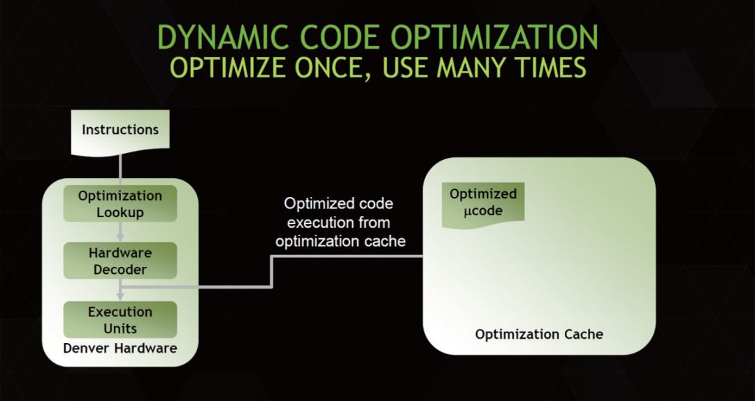
Ultimately, in various tests and industry discussions, it was found that Denver did not possess any extraordinary capabilities; in terms of the processor’s front-end decoding engine, Denver only had 2 decoding ports, making it a traditional dual-issue processor. However, in subsequent instruction processing, NVIDIA cleverly utilized dynamic instruction optimization technology, equipping a 128KB instruction cache after the dual-issue hardware decoding ports to store decoded instructions that had undergone “execution order optimization” and then packaging them into a VLIW instruction bundle for one-time transmission to the back-end processing unit, corresponding to 7 execution units internally. This is likely the true process behind NVIDIA’s claim that Denver adopts a 7-wide front end or “7-way Superscalar” architecture.
Subsequently, in the Tegra X2, which is the SoC used for DRIVER PX2, NVIDIA introduced the Denver 2 architecture. The Tegra X2 combines 2 Denver 2 architecture cores with 4 Cortex-A57 cores to form a heterogeneous system, mainly targeting the smart industry with very relaxed power consumption control. Additionally, the Jetson TX2 also uses this SoC. However, NVIDIA has not provided any specific performance or architecture information about it.
In Xavier, NVIDIA integrated a brand new self-developed Carmel CPU and once again claimed that this processor has a 10-wide processing width. Clearly, like several previous generations of processors, this 10-wide width does not refer to the number of front-end hardware decoding units but rather the number of optimized instructions after reorganization. This means that Carmel likely expanded the number of back-end execution units compared to the 7-wide Denver processor, while the front-end decoding unit may maintain a dual-issue or at most 3-issue specification, which is also the current standard configuration for mainstream ARM processors.
In other specifications, Xavier also lists detailed specifications. In terms of memory, Xavier integrates an eight-channel, 256-bit LPDDR4X memory controller, with each channel supporting a maximum of 32-bit bandwidth LPDDR4X-4266 memory, achieving a maximum bandwidth of 127.1GB/s. Xavier supports PCIe 4.0, offering a maximum PCIe 4.0 x8 configuration, which can be split into x4, x2, x1, and other specifications. Xavier also supports 3 USB 3.1 and 4 USB 2.0 ports, allowing connection to many devices such as more sensors.

▲The Denver architecture adopts a special VLIW parallel method, which differs from current mainstream ARM processors.
Additionally, Xavier supports the NVLINK bus, allowing it to connect with NVIDIA’s GPUs and provide I/O consistency features, which can enhance Xavier’s capabilities in deep learning and vision processing, although the overall power consumption will also increase.
In terms of camera support, Xavier can support 16 CSI channels, with transmission speeds of 40Gbps under DPHY 1.2 specifications and 109Gbps under new CPHY 1.1 specifications. For display output, Xavier supports 4 DP, HDMI 2.0, eDP, and other interfaces, capable of outputting 4k@60Hz images while supporting DP HBR3 data rates.
After the launch of the Xavier processor, another important question emerged: how to obtain a system that matches Xavier. After all, Xavier is a processor, and it cannot be directly used for operations. Moreover, unlike products like GPUs, Xavier is aimed at a system and currently does not exist in large-scale commercial forms, making it unlikely for third-party manufacturers to launch any systems based on Xavier, as there is no profit to be made.
So, how to establish an ecological chain to support this SoC, and how to develop and research based on Xavier requires NVIDIA to launch corresponding development templates or systems, making it easier for developers to operate. In this context, NVIDIA has launched the Jetson AGX Xavier, a mature small computer or embedded system based on Xavier, equipped with almost all interfaces, power, and functional modules, allowing users to quickly get started and understand and utilize Xavier’s features.
Visually, the Jetson AGX Xavier is a small box surrounded by a black heat sink, with various interfaces around it. The visible external interfaces include network, HDMI, USB 3.1, MIPI CSI-2 for connecting cameras, and a 40-pin GPIO interface.
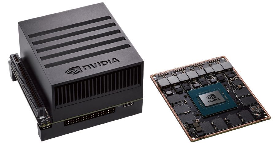
▲Appearance of Jetson AGX Xavier, a black box.
It is also worth mentioning that Jetson AGX provides a PCIe 4.0 X16 slot and an M.2 PCIe X1 slot, which is very rare on typical ARM architecture development boards, as PCIe control is complex and takes up a lot of space; typical ARM SoCs do not have extra PCIe lanes available. In terms of power, Jetson AGX provides a 64W LiteOn power supply, using 19V power, and its appearance is quite similar to that of a laptop charger.
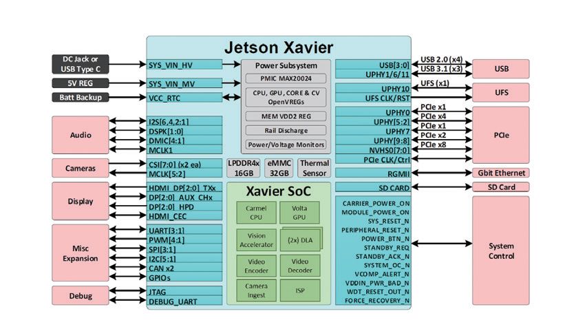
▲Jetson AGX Xavier’s architecture and connection capabilities
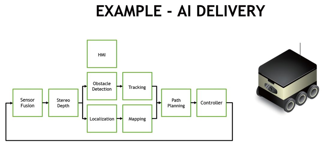
In terms of specifications, NVIDIA claims that Jetson AGX Xavier is the world’s first platform specifically designed for smart robots, edge computing, and other applications, suitable for deployment in situations that do not require human intervention, supporting functions such as visual odometry, sensor fusion, localization, obstacle detection, and path planning. Additionally, Jetson AGX Xavier supports three power modes: 10W, 15W, and 30W, allowing users to choose different power configurations based on their computing scenarios.
▲Jetson AGX Xavier has powerful AI computing capabilities
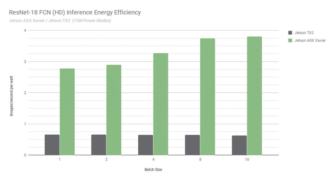
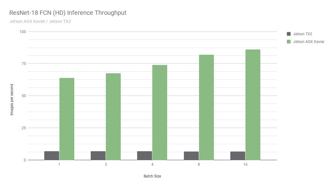
During the launch of Xavier, NVIDIA provided detailed test comparisons between Xavier and the previous TK1 and TK2, including RetsNet-18 FCN fully convolutional network tests, inference efficiency, throughput capabilities, and more. This article only briefly extracts some content.
In the RetsNet-18 FCN test, NVIDIA used a full HD model with a resolution of 2048×1024, testing for semantic segmentation to detect the perception, path planning, and navigation capabilities of autonomous computers. The performance comparison showed that thanks to Volta and the new processor architecture, Jetson AGX Xavier outperformed the previous generation products by up to 13 times, and NVIDIA stated that with software optimization and feature enhancements, performance and power advantages would further improve.
Another test based on image recognition networks ResNet-50 and VGG19 involved dividing images into 224×224 blocks for image comparison and recognition, commonly seen in some robotic platforms and automated machine camera detection. Test data indicated that in VGG19, Jetson AGX Xavier’s performance was up to 18 times higher than the previous Jetson TX2, while ResNet-50 could achieve 14 times higher throughput during testing with JetPack 4.1.1, with latency as low as 1.5 milliseconds.
NVIDIA also provided CPU performance tests for the Xavier SoC, which showed that in the CPU SPECint-Rate 8x, the Xavier SoC’s performance was about 2.5 times that of the previous Jetson TX2 using the Tegra X2 SoC, with scores of 160 compared to 61. The Tegra X2 in Jetson TX2 uses 2 Denver D15 cores paired with 4 Cortex-A57, making its overall architecture relatively old, hence the result is not surprising.
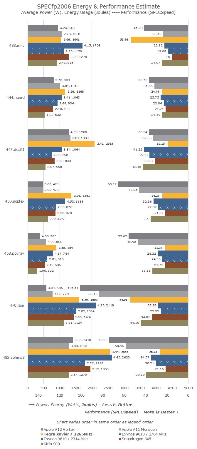
▲NVIDIA showcased extensive performance data regarding Jetson AGX Xavier and the Xavier processor
In terms of performance-to-power ratio, due to differences in process technology and target markets, for example, Jetson AGX Xavier uses a 12nm process while most mobile processors use 10nm or even 7nm processes and have stricter power consumption control, the performance-to-power ratio of Xavier is not very impressive. However, its target market does not require strict power control. From these data, the performance of the Carmel architecture adopted by Xavier is relatively normal, belonging to the mainstream level in the industry.
Xavier and Jetson AGX Xavier represent NVIDIA’s ongoing efforts in the AI market. Their launch enables more developers to leverage NVIDIA’s tools for the development and research of AI devices, including but not limited to robotics, smart vehicles, smart homes, and smart industrial control. Jetson AGX Xavier and the underlying AI technology may represent the direction of the next industrial revolution, where intelligence and AI will exponentially increase productivity, marking another major explosion in the industry. On the eve of this explosion, NVIDIA is beginning to layout its strategy, cultivating the ecological chain and system, quietly waiting for the moment to reap the benefits in the future.