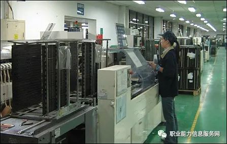
In this era of technological prosperity, LCD devices have become an indispensable part of our lives. From smartphones, televisions, and computers to watches, medical devices, and traffic lights, they all rely on the support of LCD technology. Behind this, there is a group of dedicated LCD device manufacturers who use their wisdom and hands to create a colorful display world.

The work of an LCD device manufacturer is both meticulous and complex. They need to master various skills, including optics, physics, chemistry, and electronics, while also possessing rigorous process workflows and precise operational techniques. It is the perfect combination of these skills that produces high-quality, high-performance LCD devices.
The process of manufacturing LCD devices is intricate and precise. First, manufacturers need to clean the glass substrates to ensure their surfaces are free of impurities and dust. Then, they need to coat the LCD material onto the substrates and form the LCD cells through specific processes. This process requires very precise operations because any small mistake could lead to the entire substrate being wasted.
Next, manufacturers need to package the LCD cells to protect them from external environmental interference. This process also requires a high level of professional skills and precise workflow. If the packaging is not done properly, it could lead to damage or failure of the LCD cells.
Finally, manufacturers need to conduct various tests and adjustments to ensure the performance and quality of the LCD devices meet the specified standards. This process not only requires superb skills but also patience and attention to detail. Because any negligence could lead to defects or failures in the products.
Although the work of LCD device manufacturers is arduous, they find joy in it. Because they know that through their hard work, they create high-quality, high-performance LCD devices that contribute to technological advancement. They lay the foundation for this colorful display world with their hands and wisdom.
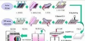
1. The manufacturing process of TFT-LCD includes the following parts
① Forming the TFT array on the TFT substrate;
② Forming the color filter pattern and ITO conductive layer on the color filter substrate;
③ Using two substrates to form the LCD box;
④ Installing peripheral circuits, assembling backlight sources, and other module assembly.
2. The process of forming the TFT array on the TFT substrate
The types of TFT that have been industrialized include: amorphous silicon TFT (a-Si TFT), polycrystalline silicon TFT (p-Si TFT), and single crystal silicon TFT (c-Si TFT). Currently, a-Si TFT is still in use.
The manufacturing process of a-Si TFT is as follows:
① First, sputter the gate material film on the borosilicate glass substrate, then form the gate wiring pattern through mask exposure, development, and dry etching. Generally, mask exposure is done using a stepper.
② Continuous film formation is performed using the PECVD method to create SiNx film, undoped a-Si film, and phosphorus-doped n+a-Si film. Then, mask exposure and dry etching are conducted to form the a-Si pattern for the TFT section.
③ A transparent electrode (ITO film) is formed using sputtering, followed by mask exposure and wet etching to create the display electrode pattern.
④ The contact hole pattern for the gate terminal insulating film is formed using mask exposure and dry etching.
⑤ Sputtering is used to form AL and other films, and mask exposure and etching are used to create the source, drain, and signal line patterns of the TFT. A protective insulating film is formed using the PECVD method, followed by mask exposure and dry etching to create the insulating film, (this protective film is used to protect the gate and signal line electrode ends and display electrode).
The TFT array process is a key part of the TFT-LCD manufacturing process and also involves significant equipment investment, requiring a very high level of cleanliness (for example, Class 10) for the entire process.

↓ScantheQRcodebelowtoquicklyregister↓
END

Scan to get more certification information!
Article edited by Beijing Qiangsheng Caishi Education Consulting Co., Ltd. If there is any infringement, please inform us for deletion