Skip to content
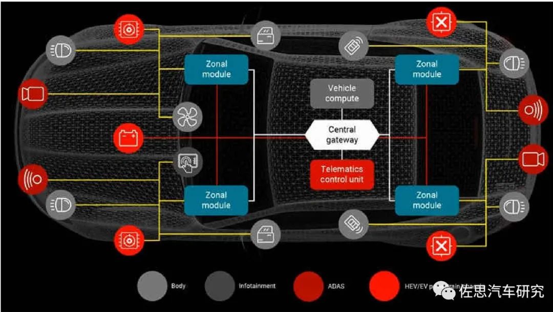
The software-defined car is inseparable from the future central computing architecture, and the two complement each other.
The above image shows the central computing architecture conceived by Texas Instruments. The author has designed a vehicle central computing architecture, choosing two NVIDIA Orin chips for the vehicle computing center, with one focusing on ADAS, named Orin A, and the other focusing on the cockpit, named Orin B.
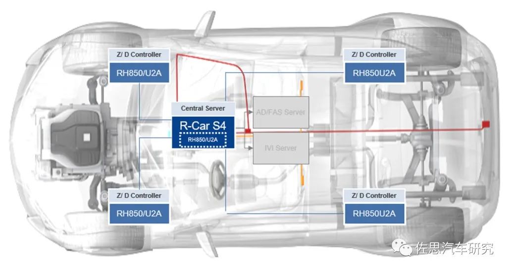
The above image shows Renesas’ central computing architecture. Since Renesas does not have the best MCU, it only depicts the MCU and the central computing center (server), which includes the AD/FAS intelligent driving server and the IVI cockpit server. For the Zonal module, it consists of sensors, actuators, and gateways; switches and MCUs actually serve as gateways. For those mainly using the CAN network, switches are unnecessary, as the CAN network is not that complex, while the Ethernet parts require Ethernet switches.
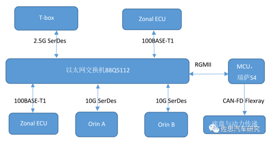 The Ethernet switch chosen is Marvell’s latest third-generation functional safety-compliant automotive Ethernet switch 88Q5112, which is a 9-port Ethernet switch. It integrates six physical layers, including three 100/10BASE-T1(S), two 1000/100BASE-T1, and one 100BASE-T1/TX. It can correspond to five Zonal ECUs plus one diagnostic OBD. The diagnostic OBD uses 1000Base-T1. Currently, apart from intelligent driving and cockpit, 100Mbps bandwidth is unnecessary; Zonal mainly serves the body and comfort networks. CAN, CAN-FD, or FlexRay is sufficient for chassis and power transfer.
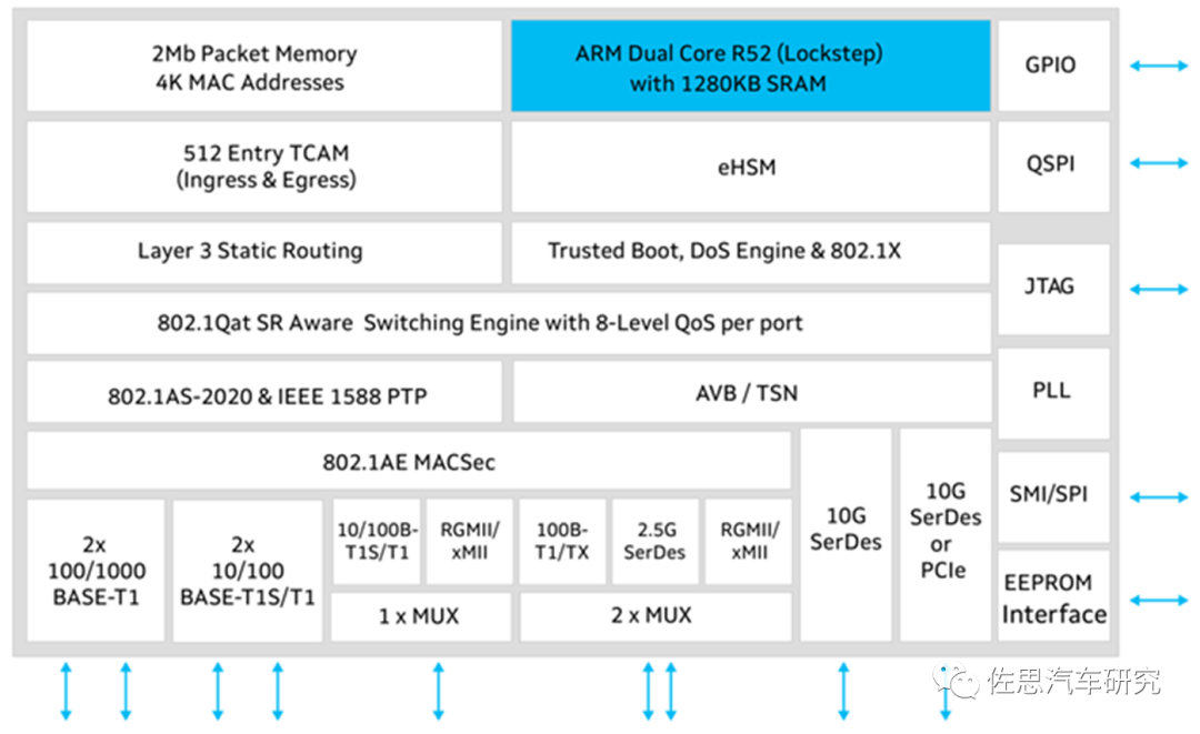
The above image shows the internal framework of the 88Q5112, which supports a rich set of TSN features, including 802.1AS-2020, 802.1Qat/Qav/Qbu/Qbv/Qci/Qcr, and ensures safety with 802.1CB.
The Ethernet switch chosen is Marvell’s latest third-generation functional safety-compliant automotive Ethernet switch 88Q5112, which is a 9-port Ethernet switch. It integrates six physical layers, including three 100/10BASE-T1(S), two 1000/100BASE-T1, and one 100BASE-T1/TX. It can correspond to five Zonal ECUs plus one diagnostic OBD. The diagnostic OBD uses 1000Base-T1. Currently, apart from intelligent driving and cockpit, 100Mbps bandwidth is unnecessary; Zonal mainly serves the body and comfort networks. CAN, CAN-FD, or FlexRay is sufficient for chassis and power transfer.
The above image shows the internal framework of the 88Q5112, which supports a rich set of TSN features, including 802.1AS-2020, 802.1Qat/Qav/Qbu/Qbv/Qci/Qcr, and ensures safety with 802.1CB.
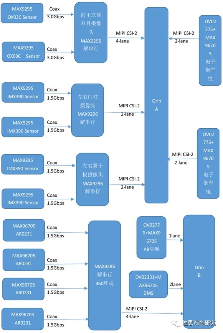 The above image shows the camera input diagram for the two Orin chips. Orin can input a maximum of 16-lane MIPI CSI-2; additionally, C-PHY and D-PHY are used for virtual channels. An 8-megapixel camera requires 4 lanes, while a camera below 2 million pixels only needs 1 lane; exceeding 2 million requires 2 lanes. For safety, 2 lanes are used for 2 million pixels, and all sensor models are for reference only. For intelligent driving, the front main camera can use three 2.5-megapixel cameras corresponding to short, medium, and long distances, or one 8-megapixel camera, or two 2.5-megapixel cameras for stereo vision. The remaining 4-6 cameras can use either 2.5-megapixel or 2-megapixel cameras. Currently, the only deserialization chip corresponding to over 2 million pixels is ADI’s MAX9296, while the serialization chip is MAX9295, which monopolizes the market. MAX9296 has adjustable rates of 1.5G, 3G, and 6G, and can handle inputs up to 16 million pixels.
The electronic rearview mirror, also known as Camera Monitor System or E-mirror, replaces the rearview mirror with a screen and requires two video inputs. Due to the small display screen, a resolution of 1 million pixels is sufficient. This display can add ADAS functions, thus falling under the ADAS system.
In the cockpit field, video inputs mainly include 360-degree surround view, AR navigation, and driver monitoring DMS. The 360-degree surround view uses a relatively advanced 2-megapixel camera and outputs to MAX9286 in a 4-in-1 format. AR navigation does not require too high a resolution, and 1.3 million pixels are sufficient. DMS is currently developing towards higher resolution, with a trend to incorporate ToF cameras, tentatively set at 2 million pixels.
Camera data can also be transmitted via Ethernet. The bitrate of a 2-megapixel camera in RAW10 format at 30fps is approximately 0.6Gbps. If it is RGB888 format, the bitrate is about 1.44Gbps, and an 8-megapixel camera has a bitrate of about 5.7Gbps. Currently, the highest Ethernet physical layer chip corresponds to 10Gbps, which can completely handle the transmission of 8-megapixel cameras. High-resolution cameras generally output in RAW8 or RAW10 format, while low-resolution cameras usually output in YUV422 format. The advantage of Ethernet transmission is that it can use a single pair of unshielded twisted pair cables, whereas MIPI CSI-2 requires coaxial cable transmission. The cost of Ethernet connectors is also significantly lower than that of MIPI CSI-2 connectors. Ethernet also facilitates data shaping and traffic control through TSN, and the communication exchange via Ethernet switch routing is more flexible than MIPI CSI-2. The cost of Ethernet physical layer chips is also lower than that of deserialization chips but higher than that of serialization chips. The downside of Ethernet is that debugging is exceptionally complex, and debugging equipment is very expensive; most engineers are not familiar with Ethernet debugging.
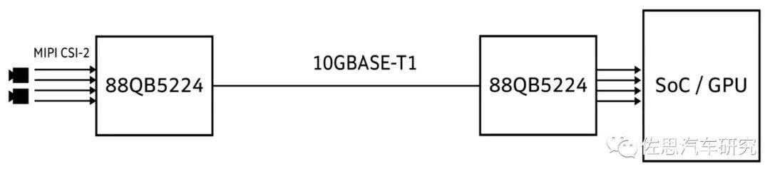
Ethernet can also bridge cameras, such as Marvell’s 88QB5224.
If the SoC’s MIPI CSI-2 interface is exhausted but cameras still need to be connected, Ethernet bridging can be considered, as shown in the image above. The 88QB5224 supports the IEEE802.3ch standard and can support up to 10G, easily connecting four 2-megapixel or 2.5-megapixel cameras.
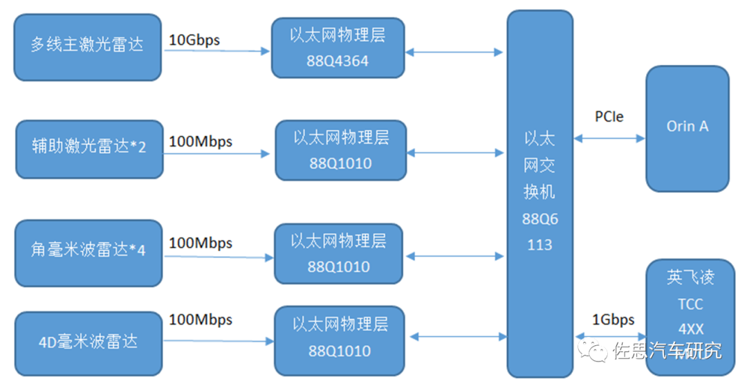
The above image shows the input cluster for LiDAR and millimeter-wave radar sensors.
LiDAR may require 1-3 units, with one main LiDAR. Considering the rapid advancement of LiDAR technology, sufficient bandwidth headroom is reserved, supporting up to 10Gbps, equivalent to the resolution of a 12-megapixel camera. Of course, LiDAR is 3D. Currently, any type of LiDAR requires 1Gbps bandwidth, which is sufficient. Auxiliary LiDAR is usually used for blind spot detection, with very low resolution; 100Mbps bandwidth is sufficient. Corner radar generally uses millimeter-wave radar, which currently mostly outputs via CAN-FD. However, it will be troublesome for Orin to support CAN-FD, so Ethernet is also used; corner radar generally supports Ethernet output, usually requiring 10Mbps bandwidth. 4D millimeter-wave radar outputs a large amount of data, and 100Mbps bandwidth is also sufficient. Finally, the MCU controlling the chassis chooses Infineon’s latest TCC4XX series, with 1Gbps bandwidth being sufficient.
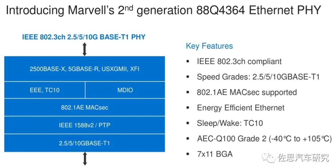
Marvell’s 88Q4364 is currently one of only two physical layer chips supporting 10G automotive Ethernet along with Broadcom’s BCM8989X.
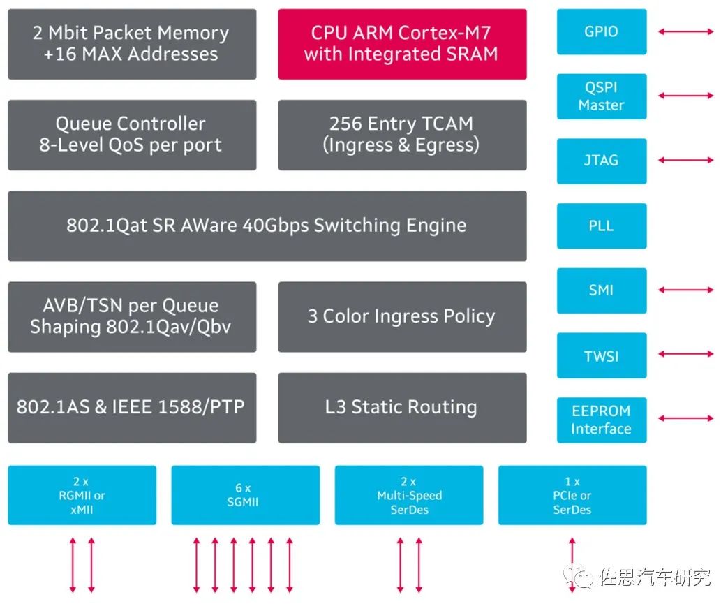
88Q6113 is Marvell’s latest third-generation 11-port Ethernet switch.
The above image shows the internal framework of the 88Q6113, which supports TSN features such as 802.1Qav/Qbv, 802.1Qat, and 802.1AS.
The above image shows the camera input diagram for the two Orin chips. Orin can input a maximum of 16-lane MIPI CSI-2; additionally, C-PHY and D-PHY are used for virtual channels. An 8-megapixel camera requires 4 lanes, while a camera below 2 million pixels only needs 1 lane; exceeding 2 million requires 2 lanes. For safety, 2 lanes are used for 2 million pixels, and all sensor models are for reference only. For intelligent driving, the front main camera can use three 2.5-megapixel cameras corresponding to short, medium, and long distances, or one 8-megapixel camera, or two 2.5-megapixel cameras for stereo vision. The remaining 4-6 cameras can use either 2.5-megapixel or 2-megapixel cameras. Currently, the only deserialization chip corresponding to over 2 million pixels is ADI’s MAX9296, while the serialization chip is MAX9295, which monopolizes the market. MAX9296 has adjustable rates of 1.5G, 3G, and 6G, and can handle inputs up to 16 million pixels.
The electronic rearview mirror, also known as Camera Monitor System or E-mirror, replaces the rearview mirror with a screen and requires two video inputs. Due to the small display screen, a resolution of 1 million pixels is sufficient. This display can add ADAS functions, thus falling under the ADAS system.
In the cockpit field, video inputs mainly include 360-degree surround view, AR navigation, and driver monitoring DMS. The 360-degree surround view uses a relatively advanced 2-megapixel camera and outputs to MAX9286 in a 4-in-1 format. AR navigation does not require too high a resolution, and 1.3 million pixels are sufficient. DMS is currently developing towards higher resolution, with a trend to incorporate ToF cameras, tentatively set at 2 million pixels.
Camera data can also be transmitted via Ethernet. The bitrate of a 2-megapixel camera in RAW10 format at 30fps is approximately 0.6Gbps. If it is RGB888 format, the bitrate is about 1.44Gbps, and an 8-megapixel camera has a bitrate of about 5.7Gbps. Currently, the highest Ethernet physical layer chip corresponds to 10Gbps, which can completely handle the transmission of 8-megapixel cameras. High-resolution cameras generally output in RAW8 or RAW10 format, while low-resolution cameras usually output in YUV422 format. The advantage of Ethernet transmission is that it can use a single pair of unshielded twisted pair cables, whereas MIPI CSI-2 requires coaxial cable transmission. The cost of Ethernet connectors is also significantly lower than that of MIPI CSI-2 connectors. Ethernet also facilitates data shaping and traffic control through TSN, and the communication exchange via Ethernet switch routing is more flexible than MIPI CSI-2. The cost of Ethernet physical layer chips is also lower than that of deserialization chips but higher than that of serialization chips. The downside of Ethernet is that debugging is exceptionally complex, and debugging equipment is very expensive; most engineers are not familiar with Ethernet debugging.
Ethernet can also bridge cameras, such as Marvell’s 88QB5224.
If the SoC’s MIPI CSI-2 interface is exhausted but cameras still need to be connected, Ethernet bridging can be considered, as shown in the image above. The 88QB5224 supports the IEEE802.3ch standard and can support up to 10G, easily connecting four 2-megapixel or 2.5-megapixel cameras.
The above image shows the input cluster for LiDAR and millimeter-wave radar sensors.
LiDAR may require 1-3 units, with one main LiDAR. Considering the rapid advancement of LiDAR technology, sufficient bandwidth headroom is reserved, supporting up to 10Gbps, equivalent to the resolution of a 12-megapixel camera. Of course, LiDAR is 3D. Currently, any type of LiDAR requires 1Gbps bandwidth, which is sufficient. Auxiliary LiDAR is usually used for blind spot detection, with very low resolution; 100Mbps bandwidth is sufficient. Corner radar generally uses millimeter-wave radar, which currently mostly outputs via CAN-FD. However, it will be troublesome for Orin to support CAN-FD, so Ethernet is also used; corner radar generally supports Ethernet output, usually requiring 10Mbps bandwidth. 4D millimeter-wave radar outputs a large amount of data, and 100Mbps bandwidth is also sufficient. Finally, the MCU controlling the chassis chooses Infineon’s latest TCC4XX series, with 1Gbps bandwidth being sufficient.
Marvell’s 88Q4364 is currently one of only two physical layer chips supporting 10G automotive Ethernet along with Broadcom’s BCM8989X.
88Q6113 is Marvell’s latest third-generation 11-port Ethernet switch.
The above image shows the internal framework of the 88Q6113, which supports TSN features such as 802.1Qav/Qbv, 802.1Qat, and 802.1AS.
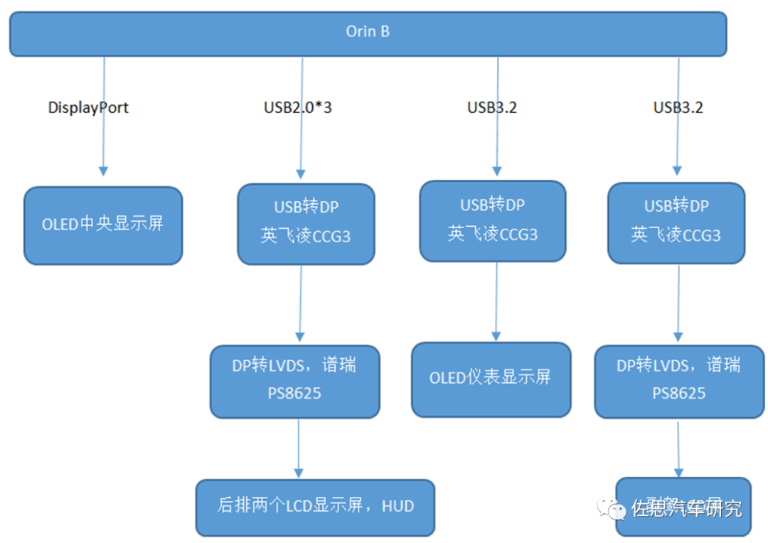 The above image shows the video output cluster of Orin B. Orin’s display output consists only of DisplayPort (DP) 1.4a, which can also be configured as HDMI output or eDP output. However, Orin has up to seven USB outputs, including three USB3.2 and four USB2.0. USB and DisplayPort can be easily converted, and then DisplayPort can be converted into other formats. Currently, high-resolution displays mainly use DP or eDP input, but in the automotive field, LVDS is still the primary input format, and the development direction is towards eDP input, as seen in the current 2K or 4K automotive OLED screens. This saves a lot of format conversion; DP can also be converted to LVDS, such as the chip used by Tesla, PS8625, which supports a maximum bandwidth of 2.7Gbps and a maximum resolution of 1920*1200. The bandwidth of USB2.0 is relatively low and can only support small screens in the back seat with a resolution of about 1280*720, which is also sufficient for AR-HUD. USB3.2 is sufficient to support 2K resolution. With Orin’s powerful GPU capabilities, outputting to five 2K displays should be quite manageable. Orin A also requires three video outputs: one to transmit to the central display CID, which can manually switch the signal source using Orin A’s DP output, and the other two are electronic rearview mirrors, using Orin’s USB3.2 output converted to LVDS.
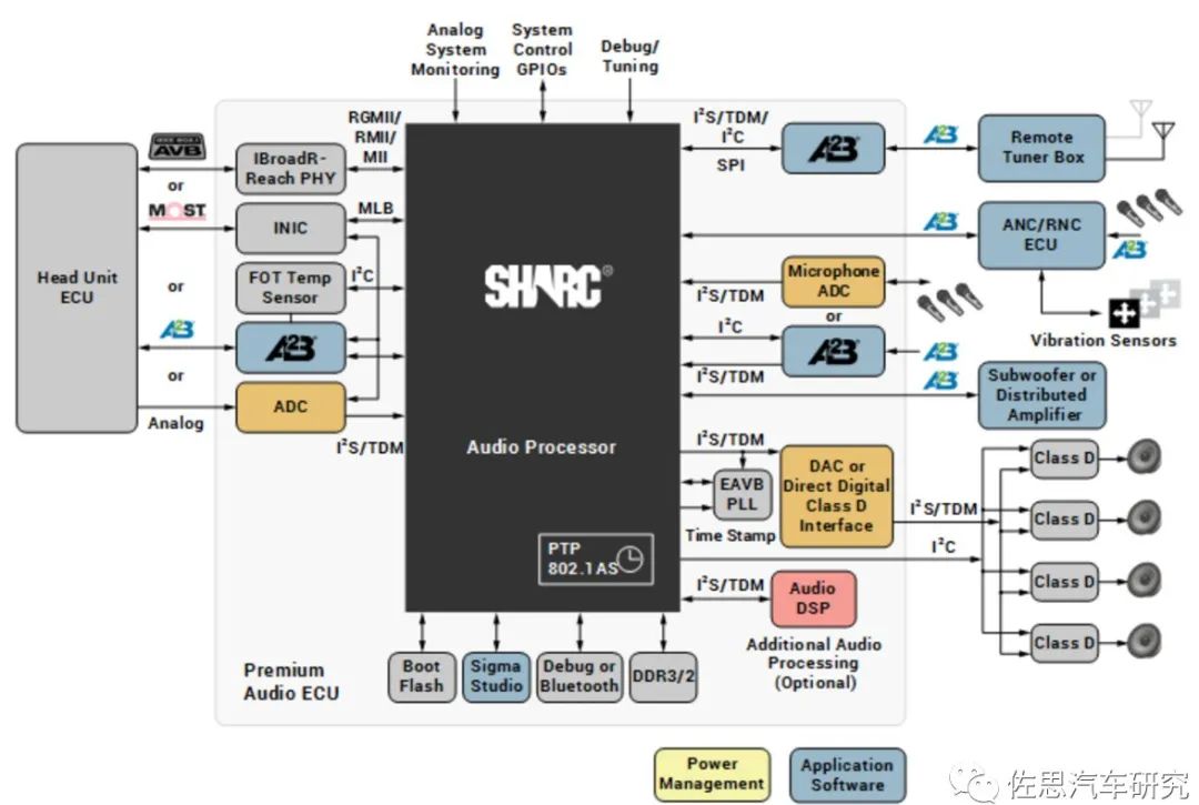 The audio section of the cockpit can refer to ADI’s design, which is top-notch cabin audio and includes active noise cancellation inside the car and road noise cancellation. A key premise for good sound quality is low cabin noise. The HeadUnit is Orin B, and the outdated MOST bus requires fiber optics, which is very troublesome and has already been abandoned by the times. The diagram also lacks a branch to the T-Box for E-Call.
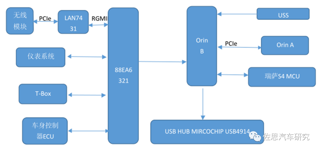 The above image shows the peripherals of the cockpit. Generally, the SoC’s PCIe port connects to the PCIe of Bluetooth and WiFi wireless modules, but the two Orins will occupy the highest level of PCIe. Additionally, board-to-board connections sometimes also use PCIe, so an additional PCIe to Ethernet converter using MICROCHIP’s LAN7431 is designed. The Ethernet switch chosen is the 7-port 88EA6321. Many of Orin’s USB interfaces are occupied, so a USB HUB, MICROCHIP’s USB4914, is needed. The MCU for the cockpit still chooses Renesas S4 or the traditional RH850. USS refers to ultrasonic sensors, which generally connect using the DSI3 bus, with one master and eleven slaves. The ultrasonic sensor system can connect to Orin using UART+SPI, which is relatively cumbersome.
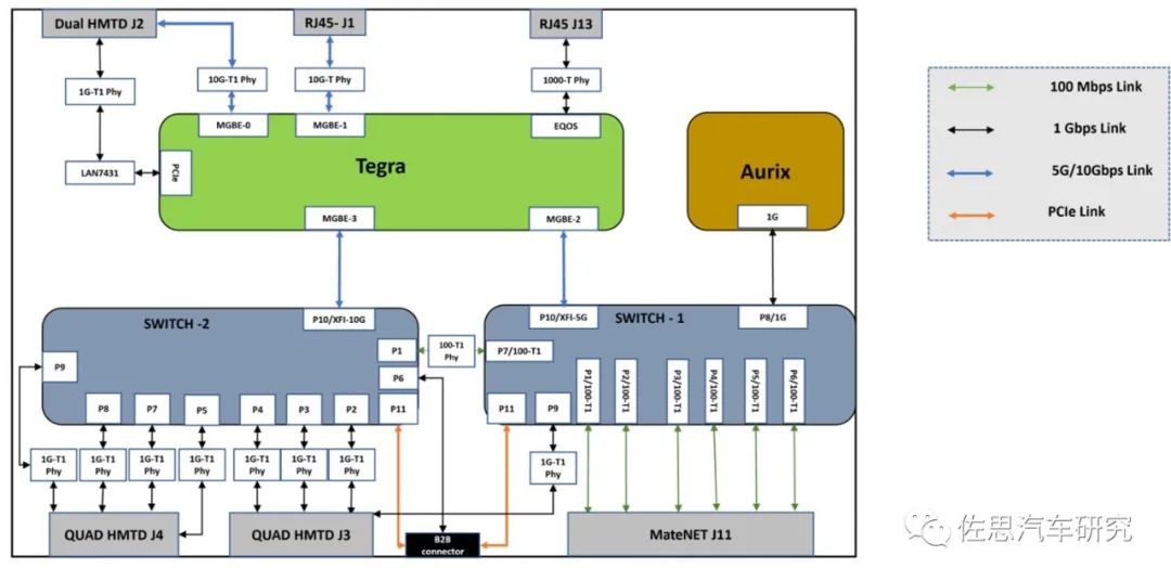
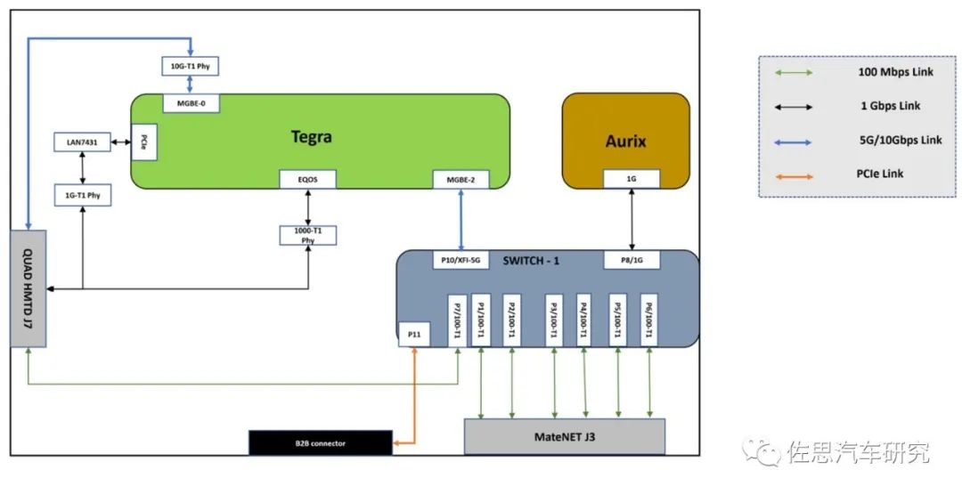
NVIDIA DRIVE 6.0 Network Topology Safety Mode
Finally, here is the network topology diagram of NVIDIA’s latest autonomous driving system DRIVE 6.0 for reference. DRIVE 6.0’s network topology has two modes: BASE and Safety, with the above image showing the Safety mode. In Safety mode, the CPU of the Ethernet switch is bypassed, so OTA is not supported. At the same time, the maximum MTU size is reduced from 16k to 1500 bytes. Here, Tegra refers to Orin, and Aurix is Infineon’s TC397T. The Ethernet switch 1 here is Marvell’s 88Q5072, and Ethernet switch 2 is 88Q6113. LAN7431 is Microchip’s PCIe to Ethernet chip. For safety, the Safety mode sacrifices some switch performance, so an additional high-grade Ethernet switch 88Q6113 is added, while actually, one 88Q5072 would be sufficient.
NVIDIA DRIVE 6.0 Network Topology Base Mode
This is the BASE mode of DRIVE 6.0’s network topology, with the Ethernet switch being 88Q5072. Orin has two 10Gbps lines, one connecting to the Ethernet switch and the other connecting to the central gateway, which is the backbone Ethernet line inside the car.
NVIDIA also specifically mentioned the API for the in-vehicle Ethernet TSN standard, which includes time synchronization 802.1AS (gPTP), sequencing and traffic shaping 802.1Qav, 802.1Qbv, 802.1Qbu/802.3br, 802.1CB, and 802.1Qci, and fault tolerance 802.1Qat and 802.1Qcc.
The future central computing architecture is somewhat like a PC, where all data processing relies on a single CPU. The basic middleware AUTOSAR and operating systems like Linux, QNX, Android, etc., form a system similar to Windows, which is essentially transparent to most programmers; they only need to design application software. This is the true software-defined car.
The above image shows the peripherals of the cockpit. Generally, the SoC’s PCIe port connects to the PCIe of Bluetooth and WiFi wireless modules, but the two Orins will occupy the highest level of PCIe. Additionally, board-to-board connections sometimes also use PCIe, so an additional PCIe to Ethernet converter using MICROCHIP’s LAN7431 is designed. The Ethernet switch chosen is the 7-port 88EA6321. Many of Orin’s USB interfaces are occupied, so a USB HUB, MICROCHIP’s USB4914, is needed. The MCU for the cockpit still chooses Renesas S4 or the traditional RH850. USS refers to ultrasonic sensors, which generally connect using the DSI3 bus, with one master and eleven slaves. The ultrasonic sensor system can connect to Orin using UART+SPI, which is relatively cumbersome.
NVIDIA DRIVE 6.0 Network Topology Safety Mode
Finally, here is the network topology diagram of NVIDIA’s latest autonomous driving system DRIVE 6.0 for reference. DRIVE 6.0’s network topology has two modes: BASE and Safety, with the above image showing the Safety mode. In Safety mode, the CPU of the Ethernet switch is bypassed, so OTA is not supported. At the same time, the maximum MTU size is reduced from 16k to 1500 bytes. Here, Tegra refers to Orin, and Aurix is Infineon’s TC397T. The Ethernet switch 1 here is Marvell’s 88Q5072, and Ethernet switch 2 is 88Q6113. LAN7431 is Microchip’s PCIe to Ethernet chip. For safety, the Safety mode sacrifices some switch performance, so an additional high-grade Ethernet switch 88Q6113 is added, while actually, one 88Q5072 would be sufficient.
NVIDIA DRIVE 6.0 Network Topology Base Mode
This is the BASE mode of DRIVE 6.0’s network topology, with the Ethernet switch being 88Q5072. Orin has two 10Gbps lines, one connecting to the Ethernet switch and the other connecting to the central gateway, which is the backbone Ethernet line inside the car.
NVIDIA also specifically mentioned the API for the in-vehicle Ethernet TSN standard, which includes time synchronization 802.1AS (gPTP), sequencing and traffic shaping 802.1Qav, 802.1Qbv, 802.1Qbu/802.3br, 802.1CB, and 802.1Qci, and fault tolerance 802.1Qat and 802.1Qcc.
The future central computing architecture is somewhat like a PC, where all data processing relies on a single CPU. The basic middleware AUTOSAR and operating systems like Linux, QNX, Android, etc., form a system similar to Windows, which is essentially transparent to most programmers; they only need to design application software. This is the true software-defined car.