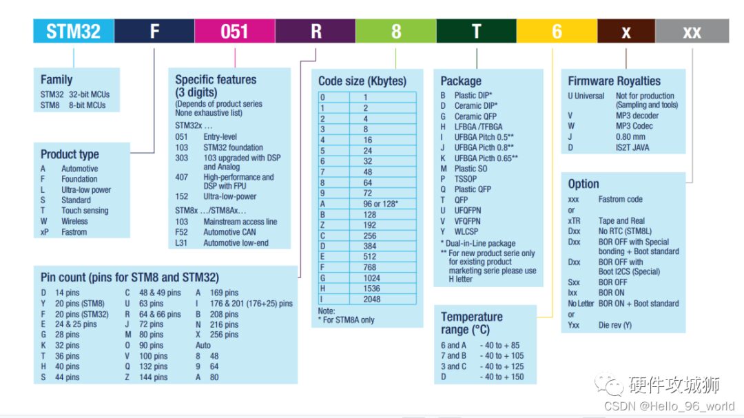
Understanding STM32
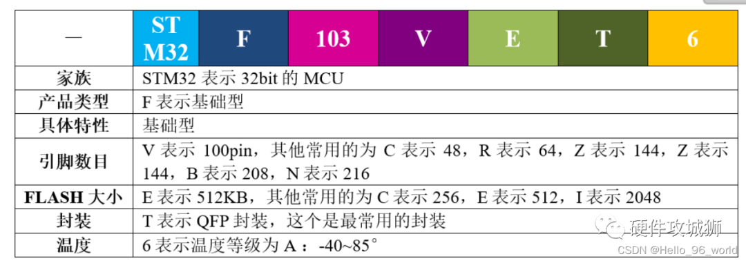 F1 represents the basic model, based on the Cortex-M3 core, with a clock frequency of 72MHZ, while F4 represents high performance, based on the Cortex-M4 core, with a clock frequency of 180M.
GPIO Peripherals
1. Eight Working Modes of GPIO
1. Pull-up Input: The IO port maintains a high level in the absence of input.
2. Pull-down Input: The IO port maintains a low level in the absence of input.
3. Floating Input: In a floating input state, the level state of the IO is uncertain and is entirely determined by external input. If the pin is left floating, reading the port level is uncertain.
4. Analog Input: The input signal is directly connected without a Schmitt trigger, and the input signal is an analog quantity rather than a digital quantity; other input methods input a digital quantity.
5. Push-Pull Output: Can output high and low levels, connecting digital devices; the push-pull structure generally refers to two transistors controlled by two complementary signals, where one transistor is always on while the other is off. The high and low levels are determined by the IC’s power supply. It has low conduction loss and high efficiency. The output can both supply current to the load and extract current from the load. The push-pull output stage improves the circuit’s load capacity and increases switching speed.
6. Open-Drain Output: The output terminal is equivalent to the collector of a transistor. To obtain a high-level state, a pull-up resistor is required. It is suitable for current-type drives, with a relatively strong current absorption capability (generally within 20mA). The open-drain circuit has the following characteristics:
(1) Utilizes the driving capability of external circuits, reducing the internal driving of the IC. When the internal MOSFET of the IC is turned on, the driving current flows from the external VCC through the pull-up resistor and MOSFET to GND. The IC only requires a small gate driving current.
(2) Generally, open-drain is used to connect devices of different levels, used for level matching. Because the open-drain pin cannot output high level without an external pull-up resistor, if high-level output is also required, a pull-up resistor must be connected. A good advantage is that by changing the voltage of the pull-up power supply, the transmission level can be changed. For example, adding a pull-up resistor can provide TTL/CMOS level output, etc. (The resistance value of the pull-up resistor determines the speed of logic level conversion. The larger the resistance value, the slower the speed and the lower the power consumption, so the choice of load resistance should balance power consumption and speed.)
(3) Open-drain output provides a flexible output method, but it also has its weaknesses, which bring rise time delays. Because the rise time is charged through the external pull-up passive resistor to the load, if the resistance is small, the delay is small but power consumption is large; conversely, the delay is large but power consumption is small. Therefore, if there are requirements for delay, it is recommended to use falling edge output.
(4) Multiple open-drain outputs can be connected to one line. By using a pull-up resistor, without adding any devices, a “wired AND” relationship can be formed. It can be simply understood as follows: when all pins are connected together, an external pull-up resistor is connected, if one pin outputs a logic 0, it is equivalent to grounding, and the parallel loop is “equivalent to being shorted by a wire”; thus the external circuit logic level becomes 0, only when all are high levels, the result is logic 1.
7. Multiplexed Push-Pull Output: At this time, the IO is controlled by internal peripherals, such as the PWM of the timer, such as SPI’s MOSI, MISO, etc. Ordinary push-pull outputs are controlled by ODR.
8. Multiplexed Open-Drain Output: Refer to multiplexed push-pull.
2. Summary of IO Mode Selection in STM32
1. Floating Input GPIO_IN_FLOATING – Floating input, can be used for KEY recognition, RX1.
2. Pull-up Input GPIO_IPU – IO internal pull-up resistor input.
3. Pull-down Input GPIO_IPD – IO internal pull-down resistor input.
4. Analog Input GPIO_AIN – Used for ADC analog input, or low power consumption to save energy.
5. Open-Drain Output GPIO_OUT_OD – IO outputs 0 to GND, IO outputs 1, floating, an external pull-up resistor is required to achieve high-level output. When the output is 1, the state of the IO port is pulled high by the pull-up resistor, but since it is in open-drain output mode, the IO port can also be changed to low level or remain unchanged by external circuits. The IO input level change can be read to achieve the bidirectional function of C51’s IO.
6. Push-Pull Output GPIO_OUT_PP – IO outputs 0 to GND, IO outputs 1 to VCC, reading input values is uncertain.
7. Multiplexed Push-Pull Output GPIO_AF_PP – Internal peripheral functions (I2C’s SCL, SDA).
8. Multiplexed Open-Drain Output GPIO_AF_OD – Internal peripheral functions (TX1, MOSI, MISO, SCK, SS).
RCC Clock
The main function of the RCC clock: set the system clock SYSCLK, set the AHB prescaler (which determines how much HCLK equals), set the APB2 prescaler (which determines how much PCLK2 equals), set the APB1 prescaler (which determines how much PCLK1 equals), set the prescaler for each peripheral; control the enabling of the clocks for AHB, APB2, and APB1 buses, and control the enabling of each peripheral’s clock. The configuration of these four clocks is generally: PCLK2 = HCLK = SYSCLK = PLLCLK = 72M, PCLK1 = HCLK/2 = 36M. (Taking STM32F103VET6 as an example)
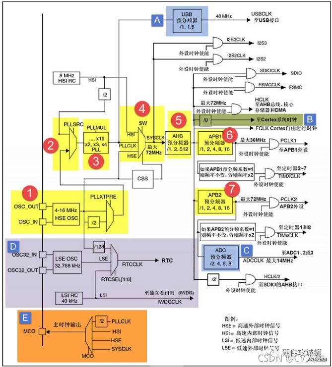
Using HSE, the steps to set the system clock are:
* 1. Enable HSE and wait for HSE to stabilize.
* 2. Set the AHB, APB2, and APB1 prescalers.
* 3. Set the PLL clock source and the PLL multiplication factor; this is where various frequencies are mainly set.
* 4. Enable PLL and wait for PLL to stabilize.
* 5. Switch PLLCK to the system clock SYSCLK.
* 6. Read the clock switch status bit to ensure PLLCLK is selected as the system clock.
NVIC is the Nested Vector Interrupt Controller
1. Priority Definition
In the NVIC, there is a dedicated register: Interrupt Priority Register NVIC_IPRx, used to configure the priority of external interrupts. The IPR width is 8 bits, and in principle, each external interrupt can be configured with a priority of 0-255, with smaller values indicating higher priority. However, most CM3 chips are designed to be simplified, resulting in a reduction in the number of supported priority levels. In F103, only the high 4 bits are used to express priority, which are grouped into preemptive priority and sub-priority. If multiple interrupts respond simultaneously, the one with higher preemptive priority will preempt the one with lower priority. If the preemptive priority is the same, the sub-priority is compared. If both the preemptive and sub-priorities are the same, their hardware interrupt numbers are compared, with smaller numbers indicating higher priority.

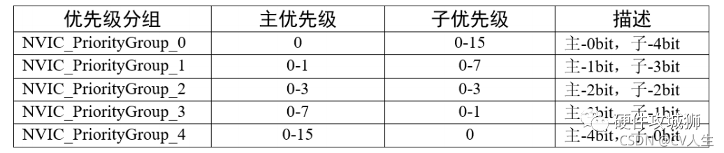
2. Priority Grouping
The grouping of priorities is determined by the PRIGROUP[10:8] bits in the Application Interrupt and Reset Control Register AIRCR of the SCB external peripheral of the core. F103 is divided into 5 groups, specifically: main priority = preemptive priority.
EXTI External Interrupt/Event Controller
EXTI (External Interrupt/Event Controller) manages the 20 interrupt/event lines of the controller. Each interrupt/event line corresponds to an edge detector that can detect rising and falling edges of input signals. EXTI can achieve individual configuration for each interrupt/event line, allowing them to be configured as interrupts or events, as well as configuring the triggering properties of events.
SysTick System Timer
SysTick is a peripheral in the CM3 core, embedded in the NVIC. The system timer is a 24-bit down-counter, which counts down every time for 1/SYSCLK. Generally, we set the system clock SYSCLK to 72M. When the value in the reload value register decrements to 0, the system timer generates an interrupt and repeats this process.
Basic Concepts of Communication
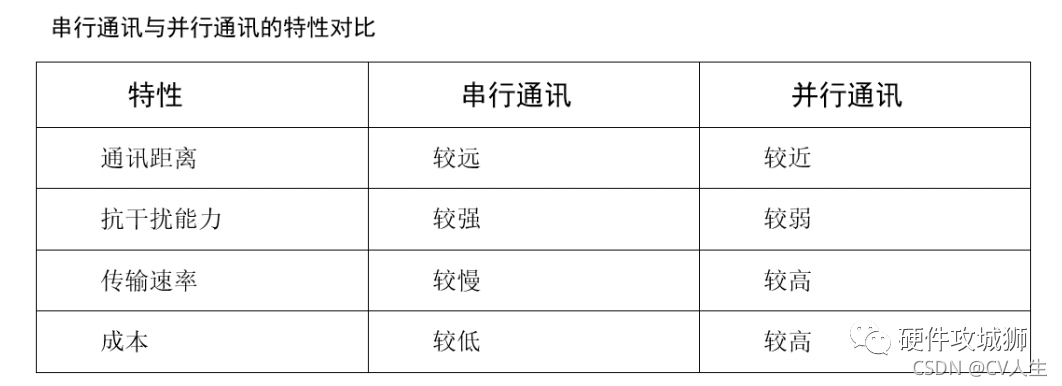
1. Serial Communication and Parallel Communication
Based on the method of data transmission, communication can be divided into serial communication and parallel communication. Serial communication refers to a method where devices transmit data bit by bit through a small number of data signal lines (generally fewer than 8), ground lines, and control signal lines. Parallel communication generally refers to a method that uses 8, 16, 32, or 64 or more data lines for transmission.
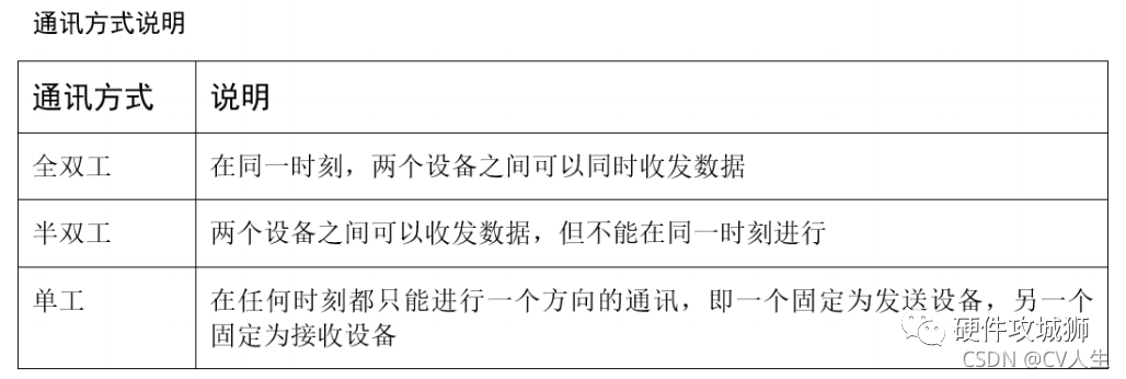
2. Full-Duplex, Half-Duplex, and Simplex Communication
According to the direction of data communication, communication can be divided into full-duplex, half-duplex, and simplex communication, primarily distinguished by the direction of the channel.
3. Synchronous Communication and Asynchronous Communication
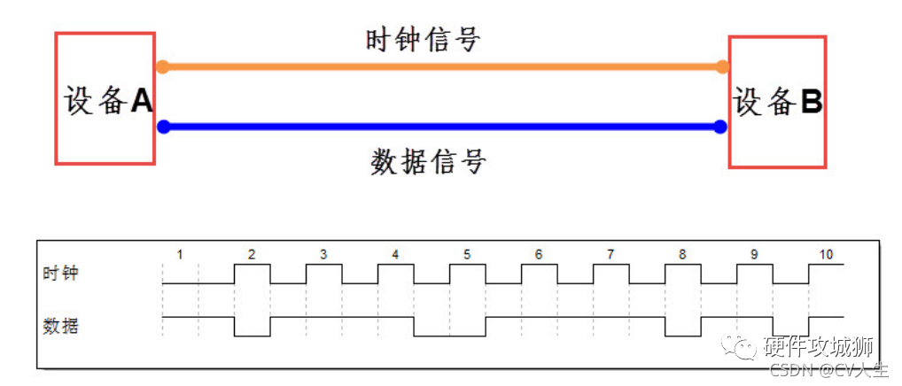
Based on the data synchronization method during communication, it can be divided into synchronous and asynchronous communication, depending on whether a clock signal is used during the communication process.
In synchronous communication, both transmitting and receiving devices use one signal line to represent the clock signal, coordinating and synchronizing data under the clock signal’s drive, as shown in the synchronous communication diagram. Typically, both parties agree to sample the data line on the rising or falling edge of the clock signal.
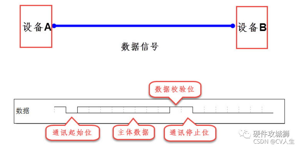
In asynchronous communication, no clock signal is used for data synchronization; instead, some synchronization bits are interspersed within the data signal, or the main data is packaged and transmitted in a data frame format, as shown in a certain asynchronous communication diagram. In some communications, both parties also need to agree on the transmission rate to better synchronize.
In synchronous communication, the content transmitted in the data signal is mostly valid data, whereas in asynchronous communication, various identifiers of the frame are included, resulting in higher efficiency for synchronous communication. However, the clock tolerance for synchronous communication is smaller than that for asynchronous communication.
4. Communication Rate
A very important parameter for measuring communication performance is the communication rate, usually expressed in bitrate (Bitrate), which indicates the number of binary bits transmitted per second, with the unit being bits per second (bit/s). A concept that is easily confused with bitrate is “baud rate” (Baudrate), which indicates the number of symbols transmitted per second. In communication, symbols with the same time interval are often used to represent a binary digit, and such signals are called symbols.
Example: In common communication transmission, 0V represents the digital 0, and 5V represents the digital 1, so one symbol can represent two states, 0 and 1; thus, one symbol equals one binary bit, and at this time, the baud rate is consistent with the bitrate. If in communication transmission, 0V, 2V, 4V, and 6V represent the binary numbers 00, 01, 10, and 11, then each symbol can represent four states, i.e., two binary bits, so the number of symbols is half the number of binary bits; thus, the baud rate is half the bitrate. Because in many common communications, one symbol represents two states, people often directly use baud rate to represent bitrate.
Serial Communication
1. Physical Layer:
The physical layer of serial communication has many standards and variants; we mainly explain the RS-232 standard.
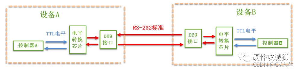
According to the different voltage standards used in communication, serial communication can be divided into TTL standard and RS-232 standard.
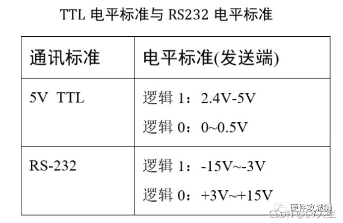
TTL voltage standard ideally uses 5V to represent binary logic 1 and 0V to represent logic 0; to increase the long-distance transmission and anti-interference capability of serial communication, it uses -15V to represent logic 1 and +15V to represent logic 0, which is RS232.
Since controllers generally use TTL voltage standards, the MA3232 chip is often used to convert signals between TTL and RS-232 voltage.
In other industrial control uses of serial communication, generally only RXD, TXD, and GND three signal lines are used to directly transmit data signals, while RTS, CTS, DSR, DTR, and DCD signals are cut off.
2. Protocol Layer
The data packet of serial communication is transmitted from the sending device through its TXD interface to the receiving device’s RXD interface. In the protocol layer of serial communication, the content of the data packet is specified, consisting of a start bit, main data, a parity bit, and a stop bit. Both parties in the communication must agree on the data packet format to send and receive data normally.
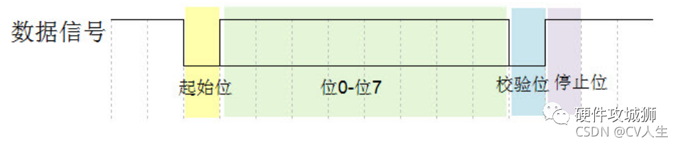
Baud Rate: In asynchronous serial communication, since there is no clock signal (as explained earlier, the DB9 interface does not have a clock signal), both communicating devices need to agree on the baud rate, i.e., the length of each symbol, to decode the signals. In the basic composition of the serial data packet, each dashed line represents one symbol. Common baud rates are 4800, 9600, 115200, etc.
The start and stop signals of communication: A data packet in serial communication starts with a start signal and ends with a stop signal. The start signal of the data packet is represented by a data bit of logic 0, while the stop signal can be represented by 0.5, 1, 1.5, or 2 data bits of logic 1.
Valid Data: Immediately following the start bit of the data packet is the main data content to be transmitted, also known as valid data, with a length commonly agreed to be 5, 6, 7, or 8 bits long.
Data Parity: After valid data, there is an optional parity bit. Since data communication is relatively susceptible to external interference leading to transmission errors, a parity bit can be added during transmission to solve this problem. Parity methods include odd parity, even parity, space parity, mark parity, and no parity.
I2C
The I2C communication protocol (Inter-Integrated Circuit) was developed by Philips. Due to its fewer pins, simple hardware implementation, strong scalability, and no need for external transceivers like USART or CAN communication protocols.
1. Physical Layer
1. Common connection methods between I2C communication devices:

Its physical layer has the following characteristics:
(1) It is a bus that supports multiple devices. A “bus” refers to a signal line shared by multiple devices. In an I2C communication bus, multiple I2C communication devices can be connected, supporting multiple communication masters and multiple communication slaves.
(2) An I2C bus uses only two bus lines, one bidirectional serial data line (SDA) and one serial clock line (SCL). The data line is used to represent data, and the clock line is used for data transmission synchronization.
(3) Each device connected to the bus has a unique address, which the master can use to access different devices.
(4) The bus is connected to the power supply through a pull-up resistor. When I2C devices are idle, they output a high-impedance state, and when all devices are idle and outputting high-impedance states, the pull-up resistor pulls the bus to a high level.
(5) When multiple masters use the bus simultaneously, arbitration is used to determine which device occupies the bus.
(6) It has three transmission modes: standard mode with a transmission rate of 100kbit/s, fast mode at 400kbit/s, and high-speed mode up to 3.4Mbit/s, although currently, most I2C devices do not support high-speed mode.
(7) The number of ICs connected to the same bus is limited by the maximum capacitance of the bus, which is 400pF.
2. Protocol Layer
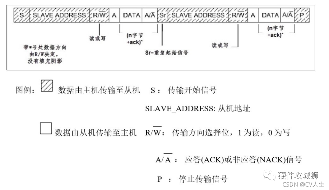
1. Basic read and write process of I2C

2. Start and stop signals of communication
When the SCL line is high, if the SDA line switches from high to low, this indicates the start of communication. When SCL is high and the SDA line switches from low to high, it indicates the stop of communication. The start and stop signals are generally generated by the master.
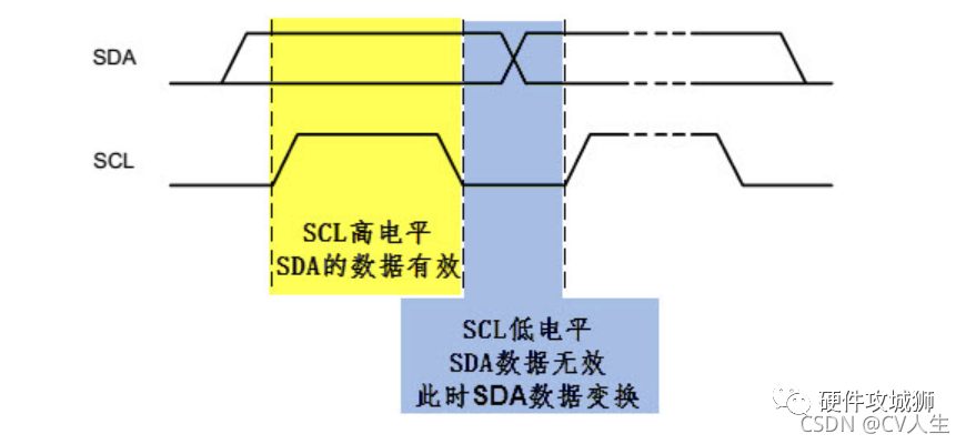
2. Data Validity
The SDA data line transmits one bit of data in each clock cycle of SCL. During transmission, when SCL is high, the data represented by SDA is valid; if SDA is high, it represents data “1”, and if low, it represents data “0”. When SCL is low, the data on SDA is invalid; generally, at this time, SDA switches levels to prepare for the next data.
Each data transmission is byte-oriented, and there is no restriction on the number of bytes transmitted each time.
3. Address and Data Direction
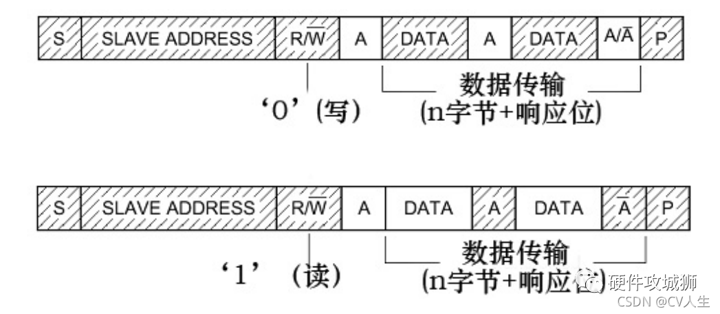
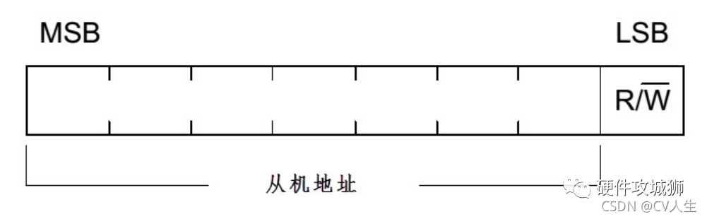
The I2C protocol specifies that the device address can be 7 bits or 10 bits long, with 7-bit addresses being more widely used in practice. Following the device address, a data bit indicates the direction of data transmission, which is the data direction bit (R/), the 8th or 11th bit. When the data direction bit is “1”, it indicates that the master reads data from the slave; when it is “0”, it indicates that the master writes data to the slave.
When reading data direction, the master releases control of the SDA signal line, allowing the slave to control the SDA signal line, and the master receives the signal. In writing data direction, the SDA is controlled by the master, and the slave receives the signal.
4. Acknowledgment
As a data receiver, when a device (whether master or slave) receives a byte of data or address transmitted via I2C, if it wishes the sender to continue sending data, it must send an acknowledgment (ACK) signal; the sender will continue to send the next data. If the receiver wishes to end the data transmission, it sends a non-acknowledgment (NACK) signal, and the sender will generate a stop signal upon receiving this signal, ending the signal transmission.
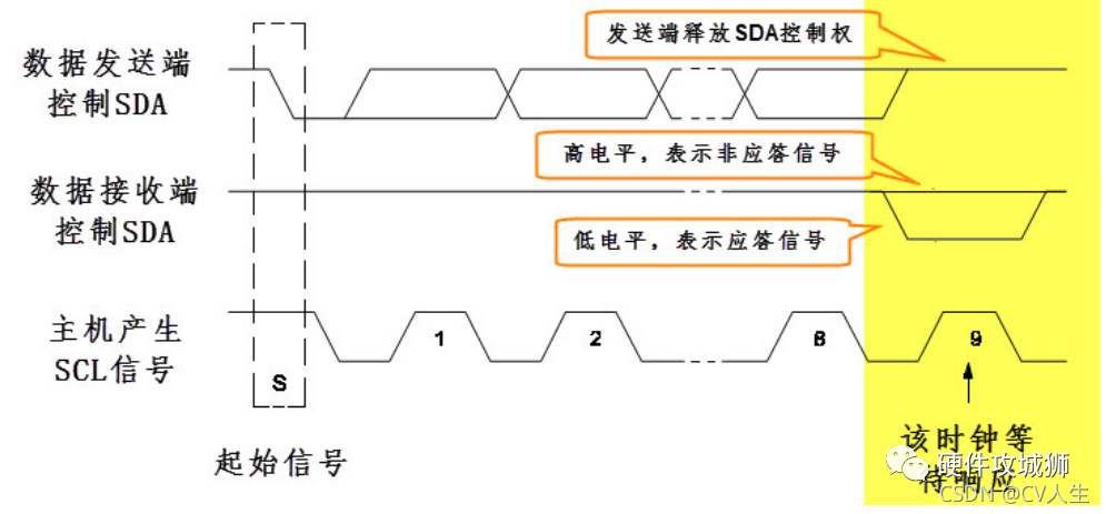
The master generates a clock during transmission, and at the 9th clock, the data sender releases control of SDA, allowing the data receiver to control SDA; if SDA is high, it indicates a non-acknowledgment signal (NACK), and low indicates an acknowledgment signal (ACK).
SPI
The SPI protocol is a communication protocol proposed by Motorola (Serial Peripheral Interface), which is a high-speed full-duplex communication bus. It is widely used in ADCs, LCDs, and other devices that require high communication rates.
1. SPI Physical Layer
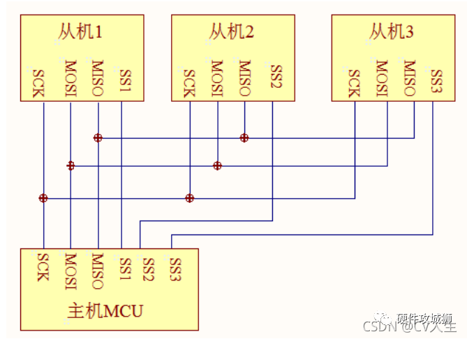
The common connection method between SPI communication devices: SPI communication uses 3 lines and a chip select line, with the three lines being SCK, MOSI, and MISO, and the chip select line NSS. (SPI communication uses the NSS line pulled low as the start signal and the NSS line pulled high as the end signal)
2. Protocol Layer
1. Communication Timing of SPI
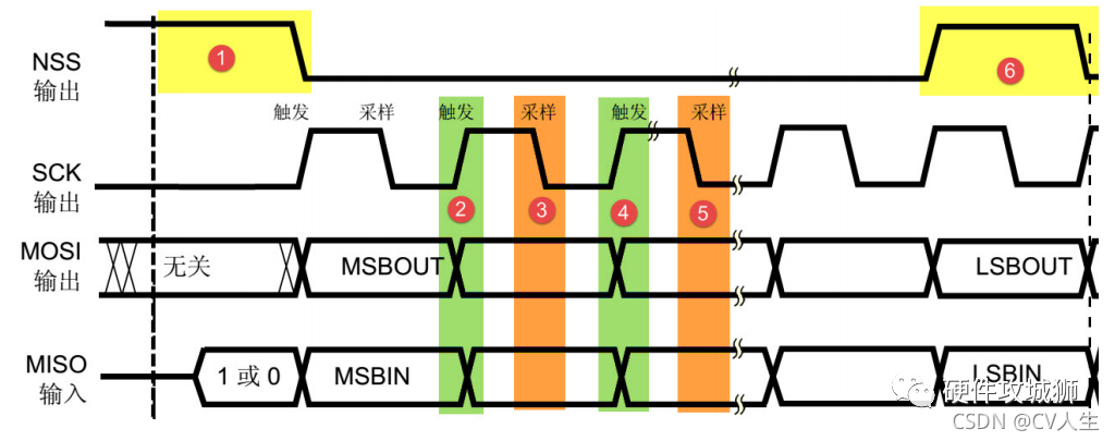
2. Start and Stop Signals of Communication
The NSS signal line changing from high to low is the start signal of SPI communication. NSS is a signal line exclusive to each slave; when a slave detects the start signal on its NSS line, it knows it has been selected by the master and begins to prepare for communication with the master. The NSS signal changing from low to high is the stop signal of SPI communication, indicating that the current communication has ended, and the slave’s selected state is canceled.
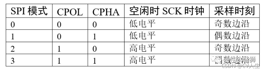
3. Data Validity
The data on the MOSI and MISO lines changes during the rising edge of SCK and is sampled during the falling edge of SCK. Thus, the data is valid when SCK is in the low state, indicating that a high level represents data “1” and a low level represents data “0”. At other times, the data is invalid, and MOSI and MISO prepare to represent the next data.
SPI transmits data in units of 8 or 16 bits each time, and there is no limit on the number of units transmitted each time.
During data transmission, whether MSB first or LSB first is not rigidly specified, but it is necessary to ensure that both SPI communication devices use the same protocol; generally, the MSB first mode shown in the SPI communication timing diagram is adopted.
DMA Direct Memory Access
DMA (Direct Memory Access) is a peripheral of the microcontroller used for data transfer without occupying the CPU, allowing the CPU to perform other tasks during data transfer, similar to multithreading. Data transfer supports from peripheral to memory or memory to memory.
The DMA controller includes DMA1 and DMA2, where DMA1 has 7 channels and DMA2 has 5 channels; here, channels can be understood as a type of data transmission pipeline. Note that DMA2 only exists in large-capacity microcontrollers.
Common Memory
1. Types of Memory
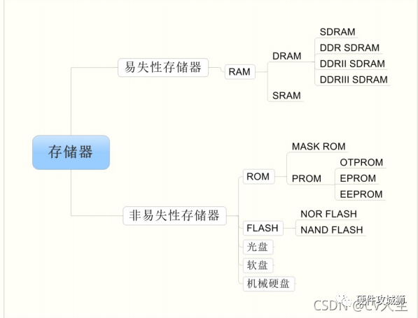
Memory can be mainly divided into “volatile memory” and “non-volatile memory” based on the characteristics of the storage medium. The terms “volatile/non-volatile” refer to whether the data stored in memory will be lost when power is cut off.
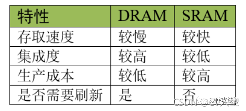
2. Volatile Memory – RAM Memory
RAM stands for “Random Access Memory”. The term “random access” means that the time required to read or write messages in memory is independent of the location of that information.
1. DRAM Dynamic Random Access Memory
DRAM’s storage units represent data with the charge of capacitors, with a charge representing 1 and no charge representing 0. However, over time, capacitors representing 1 will discharge and those representing 0 will absorb charge, thus requiring periodic refresh operations, which is what the term “dynamic” describes.
2. SRAM Static Random Access Memory
Static Random Access Memory (SRAM) uses latches to store data, as seen in the SRAM storage unit diagram. This circuit structure does not require periodic refresh charging to maintain its state (of course, if power is cut off, the data will still be lost), so this memory is called “static” RAM.
3. Non-Volatile Memory
1. ROM Memory: ROM stands for “Read Only Memory”, meaning a memory that can only be read. With technological advancements, ROMs that allow easy data writing were later designed, but the name “Read Only Memory” has been retained.
MASK ROM: MASK (Mask) ROM is the authentic “Read Only Memory”, where the data stored internally is solidified using special processes during manufacturing and cannot be modified after production, with the primary advantage being low cost during mass production.
OTPROM: OTPROM (One Time Programmable ROM) is a one-time programmable memory. This memory does not have data internally at the time of manufacture, and users can use a specialized programmer to write their data into it, but it can only be written once; once written, its content cannot be modified.
EPROM: EPROM (Erasable Programmable ROM) is a re-writable memory that solves the problem of PROM chips being writable only once. This memory uses ultraviolet light to erase data inside the chip, and both erasing and writing require specialized equipment. This type of memory has basically been eliminated and replaced by EEPROM.
EEPROM: EEPROM (Electrically Erasable Programmable ROM) is electrically erasable memory. EEPROM can be re-written, with erasing and writing directly controlled by circuitry, without needing external equipment for erasure. Moreover, data can be modified by byte, without erasing the entire chip.
2. FLASH Memory
FLASH memory, also known as flash storage, is also re-writable memory; some books refer to FLASH memory as FLASH ROM, but its capacity is generally much larger than that of EEPROM, and during erasure, it is usually done in multiple bytes. Depending on the circuit of the storage unit, FLASH memory is divided into NOR FLASH and NAND FLASH.
ADC
The STM32F103 series has 3 ADCs with a precision of 12 bits, each ADC having up to 16 external channels. ADC1 and ADC2 both have 16 external channels, while ADC3 varies in the number of external channels based on CPU pin configurations, generally having 8 external channels.
DAC
STM32 has an on-chip DAC peripheral with a resolution configurable to 8 or 12 bits of digital input signals, featuring two DAC output channels that do not affect each other, with each channel capable of using DMA functionality and having error detection capabilities, which can be externally triggered.
TIM
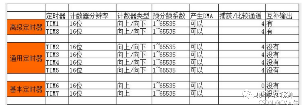
1. Classification of Timers
In the STM32F1 series, there are 8 timers in total, excluding interconnected products, divided into basic timers, general-purpose timers, and advanced timers.
IWDG Independent Watchdog / WWDG Window Watchdog
1. Definition and Usage Scenarios of Independent Watchdog
The independent watchdog is a 12-bit down-counter; when the counter’s value decreases from a certain value to 0, the system generates a reset signal, i.e., IWDG_RESET. If the counter is refreshed before it reaches 0, no reset signal will be generated, which is commonly referred to as feeding the dog.
The clock for the independent watchdog is provided by an independent RC oscillator LSI, which remains effective even if the main clock fails, making it very independent. The frequency of LSI is generally between 30~60KHZ, with some drift depending on temperature and operating conditions; we generally take it as 40KHZ, so the timing of the independent watchdog is not necessarily very precise and is only suitable for scenarios with lower time precision requirements.
2. Definition and Usage Scenarios of Window Watchdog
The window watchdog, like the independent watchdog, is also a down-counter that continuously decrements; when it reaches a fixed value of 0X40 and is not fed, it generates a reset, which is called the lower limit of the window and is a fixed value that cannot be changed. This is a similarity to the independent watchdog; the difference is that if the window watchdog’s counter value decreases to a certain number before being fed, it will also generate a reset, which is called the upper limit of the window, and this upper limit value is set independently by the user. The window watchdog’s counter value must be between the upper and lower windows to be fed.
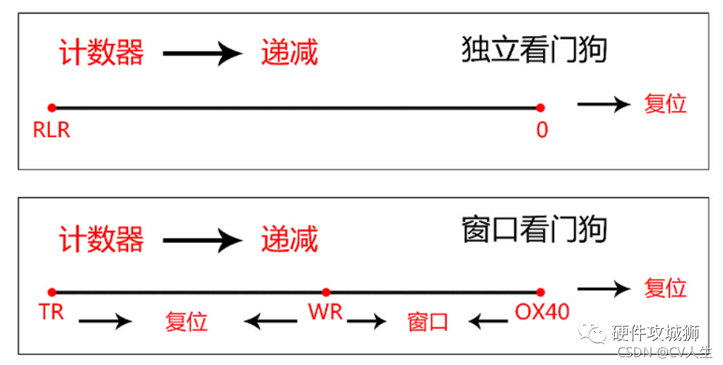
The RLR is the reload register used to set the value of the independent watchdog’s counter. TR is the counter value of the window watchdog, set independently by the user, and WR is the upper window value of the window watchdog, set independently by the user.
Original link: https://blog.csdn.net/qq_29031103/article/details/121495699