In the field of electronic design, printed circuit board (PCB) design is a complex and meticulous task. As electronic products evolve towards miniaturization and high performance, the difficulty of PCB design is increasing day by day. Among the many design tools and techniques, Boolean operations serve as a powerful graphic processing method, playing a key role in PCB design. This article will unveil the mystery of Boolean operations, analyzing their core value and practical techniques in PCB design.
What are Boolean Operations
The core idea of Boolean operations originates from set theory in mathematics, combining or cutting two or more shapes through logical relationships such as “union,” “intersection,” and “difference” to achieve complex shape combinations. In mathematics, Boolean operations mainly include basic operations like “AND,” “OR,” and “NOT,” while in graphic design and PCB design, they manifest as operations like merging, subtracting, and intersecting shapes. These operations help designers quickly construct the complex shapes they need, greatly improving design efficiency.
Boolean Operations in JLCPCB EDA Professional Version
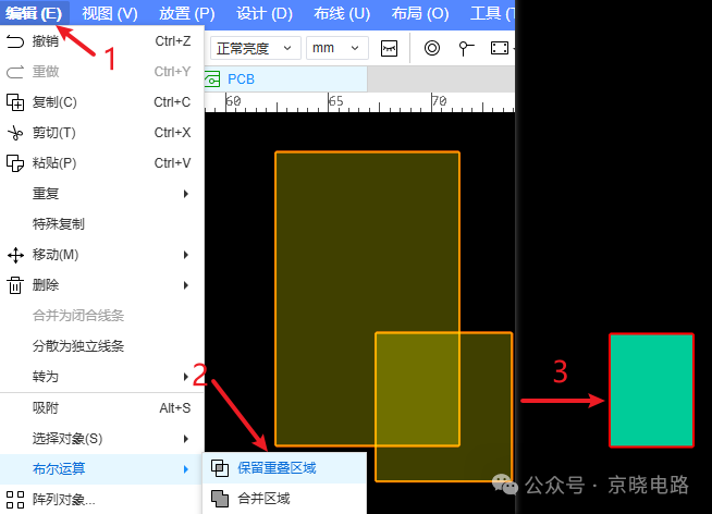
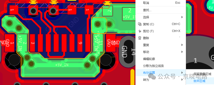
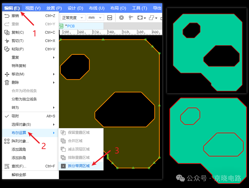
JLCPCB EDA Professional Version is a powerful PCB design software that provides users with convenient Boolean operation functions, making complex graphic operations simple and easy. By selecting the contour objects to be modified, clicking on “Edit” > “Boolean Operations” in the top toolbar, or right-clicking to find “Boolean Operations,” users can access the following five functions.
(1) Retain Overlapping Areas
In JLCPCB EDA Professional Version, after selecting the “Retain Overlapping Areas” function, the software automatically identifies the overlapping parts of the selected graphic elements and retains only that area. This function is very useful for handling overlapping parts of multiple contour areas or FPC reinforcement boards.
(2) Merge Areas
The “Merge Areas” function allows users to combine adjacent or overlapping graphic elements into a single entity. This is very helpful for simplifying the contour design of circuit boards. For example, when designing a complex polygonal circuit board, multiple small contour areas may be adjacent. By merging these areas, a more concise and regular contour can be obtained.
(3) Subtract Top Layer Areas
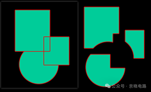
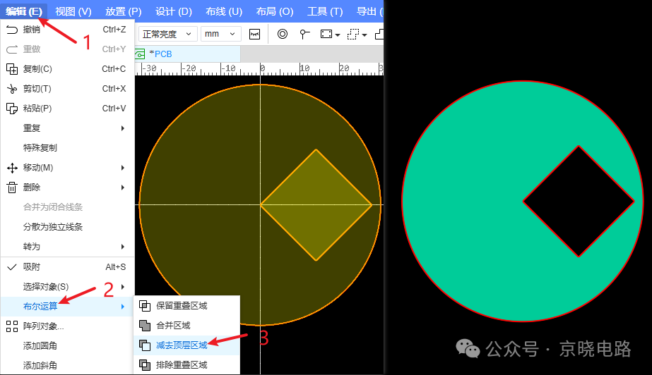
The “Subtract Top Layer Areas” function allows users to selectively subtract overlapping parts of graphic elements, currently mainly supporting filled areas. When using this function, users can select multiple graphic elements by holding down the Ctrl key and determine which part to retain based on the order of selection. The first selected graphic element will serve as the reference, and subsequent selections will be subtracted from the reference element. For example, when needing to remove a portion of a fill layer in a certain area of the circuit board, this function is very convenient.
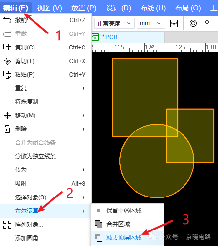
In the example below, due to the different order of selecting multiple graphic elements while holding down the Ctrl key, completely different fill shapes will be generated. Designers can decide which part to retain based on their needs. If multiple graphic elements are selected at once, the software will determine the subtraction rules based on whether the elements are completely contained or partially intersecting. This flexible operation method allows designers to precisely control the subtracted parts of the graphics, meeting various complex design requirements.
(4) Exclude Overlapping Areas
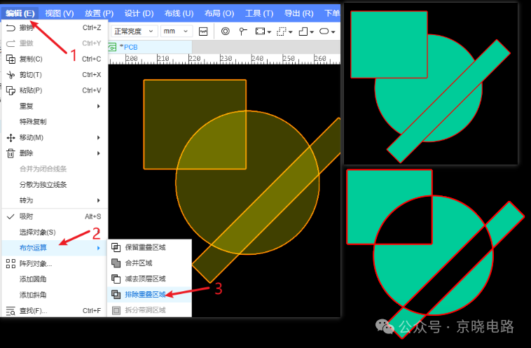
The “Exclude Overlapping Areas” function can subtract all overlapping parts of graphic elements, mainly applicable to filled areas. This function is very useful when dealing with filled areas that need to avoid overlap. For example, when designing certain special functional areas of a circuit board, it is necessary to ensure that there is no overlap between filled areas to avoid signal interference or other issues. By using the “Exclude Overlapping Areas” function, designers can easily achieve this goal, ensuring the accuracy of the design.
(5) Split Areas with Holes
The “Split Areas with Holes” function will split graphic elements with holes into a large graphic element based on the outer shape and multiple smaller graphic elements based on the shape of the holes. This function is very practical when dealing with complex hole patterns.
Conclusion
In JLCPCB EDA Professional Version, Boolean operations provide various practical functions such as retaining overlapping areas, merging areas, subtracting top layer areas, excluding overlapping areas, and splitting areas with holes. These functions offer designers flexible operation methods to meet various complex design needs. In today’s increasingly competitive environment in the electronic design field, proficient use of advanced tools like Boolean operations will help designers stand out in their work and create even better design works.
END Scan to Follow
Focusing on high-speed PCB design, quality assurance
Technical Support: Xiao Jing
 Scan to Follow
Focusing on high-speed PCB design, quality assurance
Jing Xiao Public Account