Introduction
The ADS1115 is well-suited as an introductory ΔΣ ADC for several reasons:
-
Two major players in the maker community, Adafruit and Seeedstudio, have written tutorials on its use with Raspberry Pi, see [1], [2].
-
It is included in the TI High-performance / Precision ADCs series, albeit at the lower end, as shown in Figure 1.
-
TI released its automotive version, the AEQ-100, in 2012, and the regular version was released even earlier, indicating a long product lifecycle.
-
It is affordably priced, with a unit price around 5 yuan in the Lichuang Mall, and the modules for Raspberry Pi and Arduino are also inexpensive.
-
The datasheet has been updated multiple times, providing a detailed introduction to the characteristics and typical applications of ΔΣ ADCs, see [3].
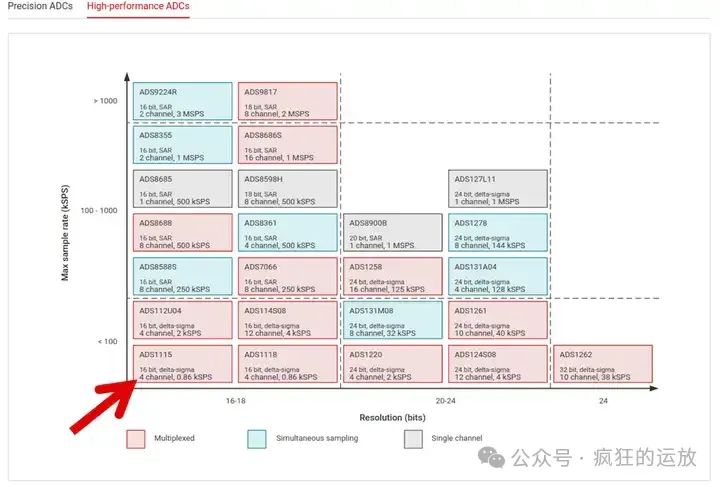
Today we will introduce this ADC, primarily based on material from the datasheet (see [3]), so this is another specification interpretation.
Overview of ADS1115
The ADS1115 is a ΔΣ ADC (Delta-sigma ADC) that includes an input MUX, PGA, reference voltage, I2C bus interface, and comparator. The block diagram is as follows:
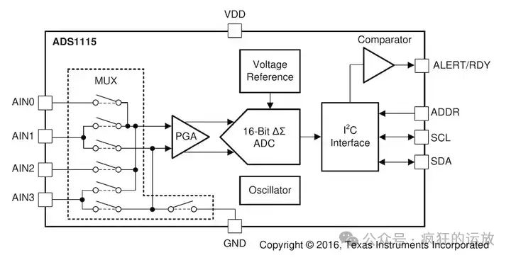
The theoretical resolution is 16 bits, with a data rate ranging from 8 SPS to 860 SPS (Samples per second), where SPS refers to the data output rate on the I2C bus. Due to the relatively low bit count and speed of the ADS1115, it ranks at the lower end in Figure 1.
The Effective Number of Bits (ENOB) is less than or equal to 16 bits, which is related to data rate, dynamic range/reference voltage, etc. The worst-case scenario occurs at the highest output rate (860 SPS) and the minimum dynamic range/reference voltage (±0.256V), yielding an ENOB of 13.8 bits, as shown in the following figure:

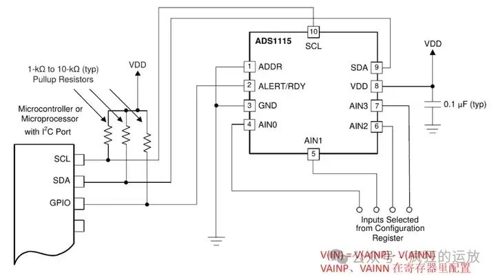
ADS1115 supports single-ended and differential inputs, where single-ended input only utilizes half of the dynamic range (FSR), while differential input uses the full dynamic range (± FSR).
Differential refers to the relative difference between AINP and AINN, which can be positive or negative, but the absolute value must be between GND and VDD, meaning it cannot be negative voltage, as indicated in the following figure:

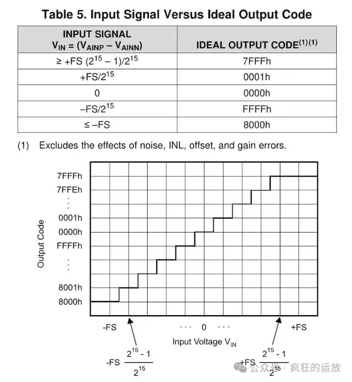
Data output is provided in 16-bit two’s complement format. The positive full-scale range (+FSR) outputs the binary code 7FFFh, and the negative full-scale range (–FSR) outputs the binary code 8000h:
That summarizes the basic information about the ADS1115.
Characteristics of Delta-Sigma (ΔΣ) ADC
Delta-Sigma (ΔΣ) ADCs are based on the principle of oversampling, where the input signal is sampled at a high modulator frequency (fMOD), followed by digital filtering and decimation, ultimately outputting the converted data at a lower rate (Data Rate).
The ratio between the modulator frequency (fMOD) and the output data rate is known as the Oversampling Ratio (OSR).
Here is a quoted segment from the datasheet:
Delta-sigma (ΔΣ) ADCs are based on the principle of oversampling. The input signal of a ΔΣ ADC is sampled at a high frequency (modulator frequency) and subsequently filtered and decimated in the digital domain to yield a conversion result at the respective output data rate.
The ratio between modulator frequency and output data rate is called oversampling ratio (OSR). By increasing the OSR, and thus reducing the output data rate, the noise performance of the ADC can be optimized.
In other words, the input-referred noise drops when reducing the output data rate because more samples of the internal modulator are averaged to yield one conversion result. Increasing the gain also reduces the input-referred noise, which is particularly useful when measuring low-level signals.
The frequency at which the input signal is sampled is called the sampling frequency or the modulator frequency (fMOD). The ADS111x has a 1-MHz internal oscillator that is further divided by a factor of 4 to generate fMOD at 250 kHz.
ADI has a classic diagram in its ΔΣ ADC tutorial that describes the relationship between the modulator (ΔΣ MOD), digital filter, data encoding (DEC), and output data rate (ODR), and illustrates the frequency spectrum of the input signal (In-Band Signal) and quantization noise (Quantization Noise). I find it quite useful, and here it is for your reference:
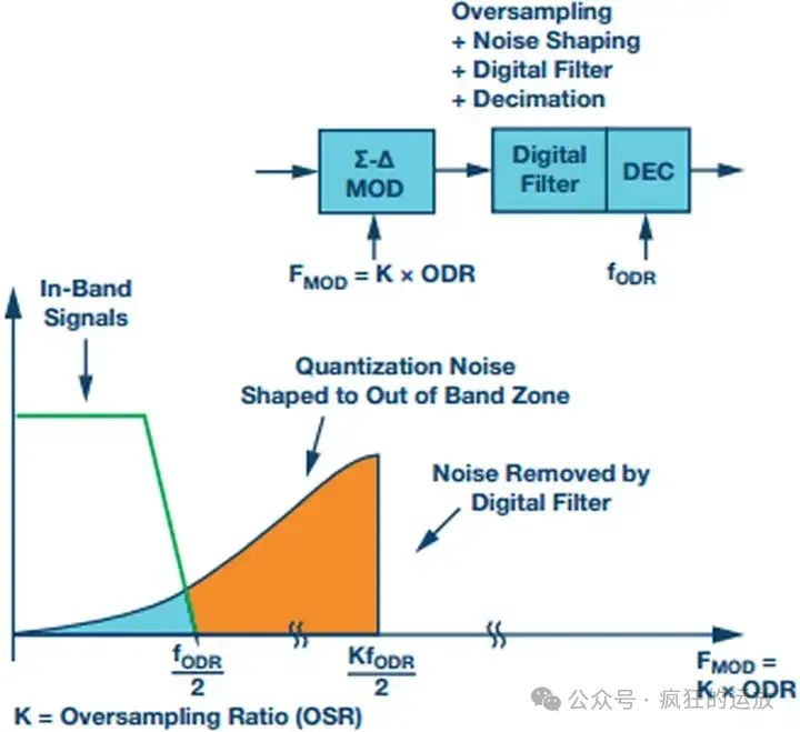
In short, ΔΣ ADCs achieve oversampling due to the high frequency fMOD, providing additional high bandwidth for noise shaping and filtering.
The datasheet illustrates the advantages of ΔΣ ADCs using a spectrum diagram:
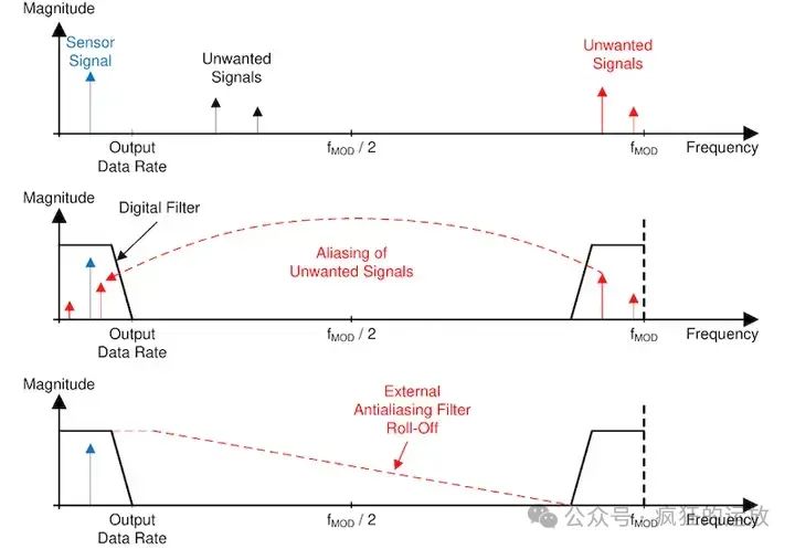
For noise (unwanted signal), after sampling at fMOD, it aliases into the Nyquist first quadrant (fMOD / 2), and then the output data rate will affect the output signal.
If an external anti-aliasing filter is added beforehand, it becomes easier to filter out this noise, and due to the high bandwidth of oversampling, this anti-aliasing filter can have a gentle roll-off.
We have discussed topics related to ΔΣ ADCs, aliasing, and oversampling in previous issues; feel free to look them up if interested.
Typical Circuit
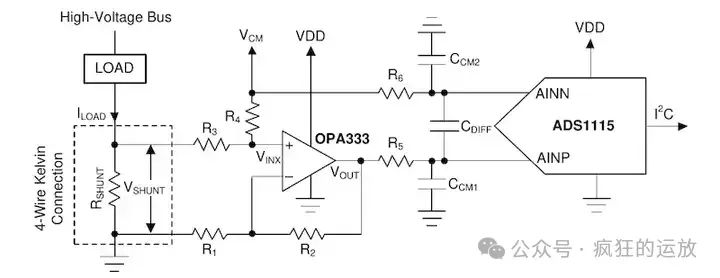
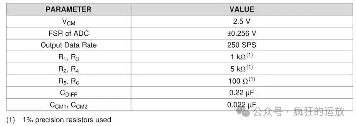
The datasheet showcases a typical circuit for measuring load current, which includes a shunt resistor (converting current to voltage), an op-amp (OPA333), ADS1115, and some filtering and voltage divider components:
Several highlights are:
-
VCM (Analog Common Mode) is connected to AINN (negative input), with VCM set to 1/2 of VDD, i.e., 2.5V;
-
AINP can be greater or smaller than AINN, thus allowing for differential input, corresponding to bidirectional flow of current;
-
The value of the shunt resistor must be reasonable to ensure a suitable dynamic range (FSR of ±0.256V);
-
The design of the resistor-capacitor components affects the input impedance and the previously mentioned external anti-aliasing filter;
I believe that such circuit designs, which incorporate many components, really test one’s foundation, requiring us to read and study datasheets and typical circuits more. Don’t you agree?
DIY Module Setup
I happen to have an ADS1115 module compatible with Raspberry Pi, aptly named ADC HAT (Hardware Attached on Top), which can be used for hands-on practice:
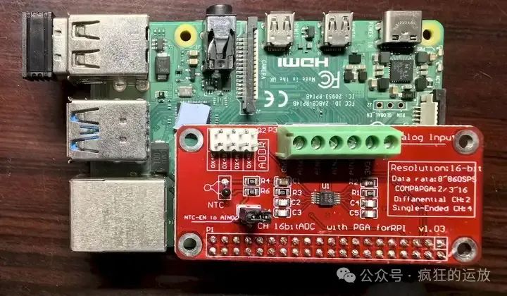
There is also an NTC temperature sensor on it, connecting the jumper cap to AIN0, and following the tutorials [1] or [2] allows data reading; the key step is to configure the Raspberry Pi’s I2C bus interface.
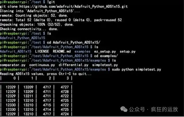
Of course, the NTC needs to convert the voltage signal back to resistance, and then back to the actual temperature.
Additionally, I see that the Raspberry Pi I2C bus speed is not very high, reportedly at 100KHz, while SPI is a bit higher [5]. However, the Raspberry Pi’s capability for handling high-frequency external interrupts should be relatively weak, possibly requiring development at the kernel level (such as DMA, Fast Interrupt, etc.). If connecting a high-speed ADC to the Raspberry Pi, it may be necessary to use ADC modules with USB or Ethernet, as these two communication methods are more convenient on Raspberry Pi.
In summary, the ADS1115’s speed is not high, but its cost-performance ratio is suitable, making it an excellent introductory module for Raspberry Pi or Arduino.
References
-
https://learn.adafruit.com/raspberry-pi-analog-to-digital-converters/
-
https://wiki.seeedstudio.com/4-Channel_16-Bit_ADC_for_Raspberry_Pi-ADS1115/
-
https://www.ti.com/product/ADS1115
-
https://www.analog.com/en/resources/technical-articles/behind-the-sigma-delta-adc-topology.html
-
https://raspberrypi.stackexchange.com/questions/108896/what-is-rpis-i2c-maximum-speed
This public account is designed for makers, providing an interesting and useful hardware and software column. Welcome to follow, like, and star~